The future of high-bandwidth memory (HBM) is set to revolutionize data centers and AI technology. New standards, including HBM4 through HBM8, promise substantial advancements to meet the rising demands of these sectors.
HBM will witness significant scaling over the next decade, driven by the growing needs of AI and data centers. These developments were unveiled by KAIST and Tera, highlighting what lies ahead for HBM technology.
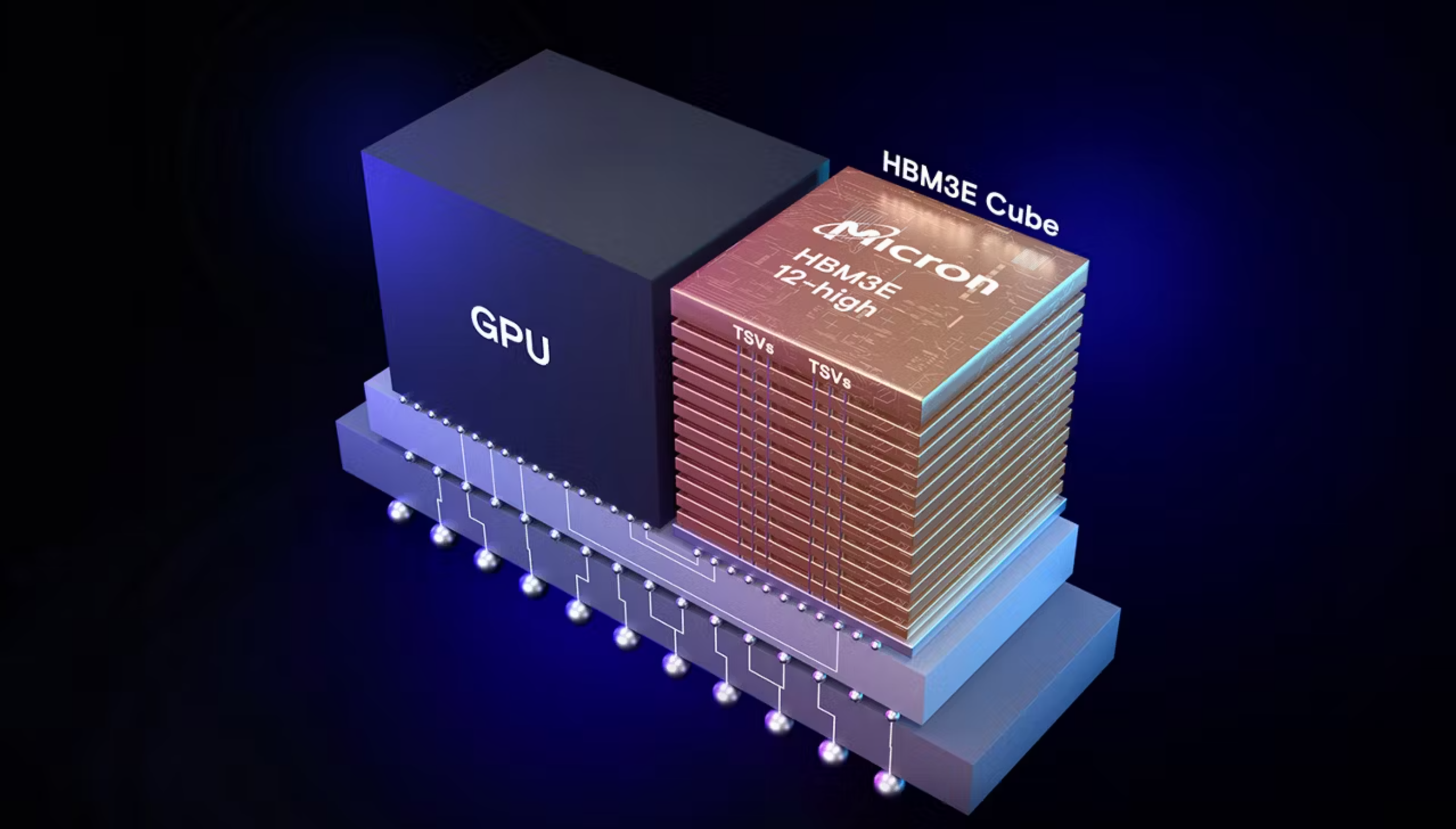
Starting with HBM4, slated for deployment in data centers and AI GPUs by 2026, it will be central to AMD and NVIDIA’s forthcoming releases. NVIDIA’s Rubin series will implement HBM4 and its enhanced version, HBM4e. Rubin will feature 8 HBM4 sites, while Rubin Ultra will double that number, offering significant compute density.
HBM4’s core features include a data rate of 8 Gbps, 2048 I/Os, and total bandwidth of 2.0 TB/s. It supports up to 24 Gb per die, reaching 36-48 GB per stack, and uses direct-to-chip liquid cooling for efficient thermal management.
Looking ahead, HBM5 aims for release in 2029. With enhanced IO lanes and increased bandwidth up to 4 TB/s, it will support 40 Gb capacity per die, reaching 80 GB per stack with advanced cooling methods like immersion cooling.
HBM6 will push boundaries further with a data rate of 16 Gbps and a total bandwidth of 8.0 TB/s. The architecture will allow 96-120 GB per stack with new bump-less bonding and advanced network integration features.
The advancement continues with HBM7 and HBM8, which will significantly enhance memory capabilities. HBM7 will deliver 24 Gbps pin speeds and massive bandwidths, supporting up to 192 GB per stack. This makes it an ideal choice for the next generation of multi-chiplet applications.
In conclusion, these next-gen HBM standards promise to not only keep up with the blistering pace of AI technological advances but also redefine what’s possible in performance and efficiency for the data centers of tomorrow.Imagine groundbreaking technology that promises an unprecedented leap in data processing and memory capacity. We’re talking about a chip that heralds the era of Exabyte-class bandwidth with a staggering 1024 TB/s. Not only does it pack a punch with an immense memory capacity ranging from 5120 to 6144 GB, depending on the HBM height, but it also demands a power input of 15,360W—nearly three times that of HBM6-based solutions.
Key innovations in the HBM8 memory standard include a striking 32 Gbps data rate, 16,384 input/output connections, and a total bandwidth of 64 TB/s. Each die stack can range from 20 to 24 layers high, boasting capacities of 200 to 240 GB per module. The packaging combines the cutting-edge Bump-Less Cu-Cu Direct Bonding with embedded cooling techniques. Advanced features like Coaxial TSV/Full-3D GPU-HBM integration, HBM-Centric Computing, and a Full Memory Network ensure it’s ready for the future.
Although HBM8 won’t hit the market until 2038, its specs already stimulate excitement. Doubling the IO lanes to 16,384 and offering 64 TB/s of stack bandwidth will revolutionize memory capacities. Each DRAM sits at 80 Gb, resulting in overall memory capacities ranging between 200 to 240 GB. With package power up to 180W per HBM site, it’s prepared to support expansive data needs.
The HBF (High-Bandwidth Flash) architecture emerges as a star, catering to memory-intensive LLM inference. This innovation swaps traditional DRAM for NAND up to 128 layers in a 16-Hi stack, interconnected through HBF TSV. A single HBF stack can add up to 1 TB of capacity and employs a rapid 2 TB/s HBM-to-HBF interconnect for seamless communication across the mainboard.
With HBM7, enhancements continue as NAND-based stacks connect to a Glass Interposer, achieving 4096 GB/s transfer speeds. A complementary LPDDR solution provides up to 384 GB of capacity, syncing with an HBM stack that offers 192 GB. HBM stacks are poised to scale up to 24-Hi designs within these high-bandwidth twin-tower packages.
Glass-based silicon interposers set the stage for the future, integrating embedded cooling that directly chills the HBM, HBF, and GPU IPs through the interposer. As these ambitious technologies unfold, anticipation builds; we’re on the edge of a memory revolution poised to redefine our digital capabilities in the years to come.