Fresh rumors suggest NVIDIA’s next-gen Rubin and Rubin Ultra AI platforms are running into meaningful design and specification hurdles, potentially giving rivals a rare opening. If these challenges linger, AMD’s upcoming MI500 accelerator family could gain an early advantage in the race to bring HBM4E-based AI systems to market in 2027.
Rubin is expected to be a major leap beyond the current Blackwell generation, with new architectures, better efficiency, and a sizeable jump in AI throughput. But multiple reports now claim the path to production isn’t as smooth as originally hoped. The talk centers on five major problem areas: HBM4 speed and capacity constraints, manufacturing yield issues, package warpage concerns, pushback tied to multi-power design choices, and late-stage changes to the heat spreader.
HBM4 speeds may be getting dialed back
One of the biggest themes is memory. Rubin is rumored to ship with 288 GB of HBM4 and up to 22 TB/s of total bandwidth. On the supply side, HBM4 production plans are already taking shape, including 12‑high (12‑Hi) stacks designed for large AI accelerators. However, the rumor mill claims NVIDIA may be struggling to validate higher-speed HBM4 operation due to base die quality concerns from memory suppliers. If that’s accurate, it can force a spec adjustment, additional validation cycles, or in a worst case, schedule pressure.
Rubin Ultra memory capacity reportedly reduced, but still massive
Rubin Ultra is where the story gets more dramatic. Early expectations pointed to as much as 1 TB of HBM4E using 16‑Hi stacks. Now, the rumored revision scales that down to 12‑Hi stacks due to yield limitations tied to volume production feasibility.
Even with the reduction, Rubin Ultra would still be enormous by today’s standards. With 16 HBM sites total (reportedly eight per GPU chiplet), a move from 16‑Hi to 12‑Hi would bring the total to around 768 GB of HBM4E—about a 25% drop versus the initial 1 TB target, but still roughly 2.66x higher capacity than standard Rubin.
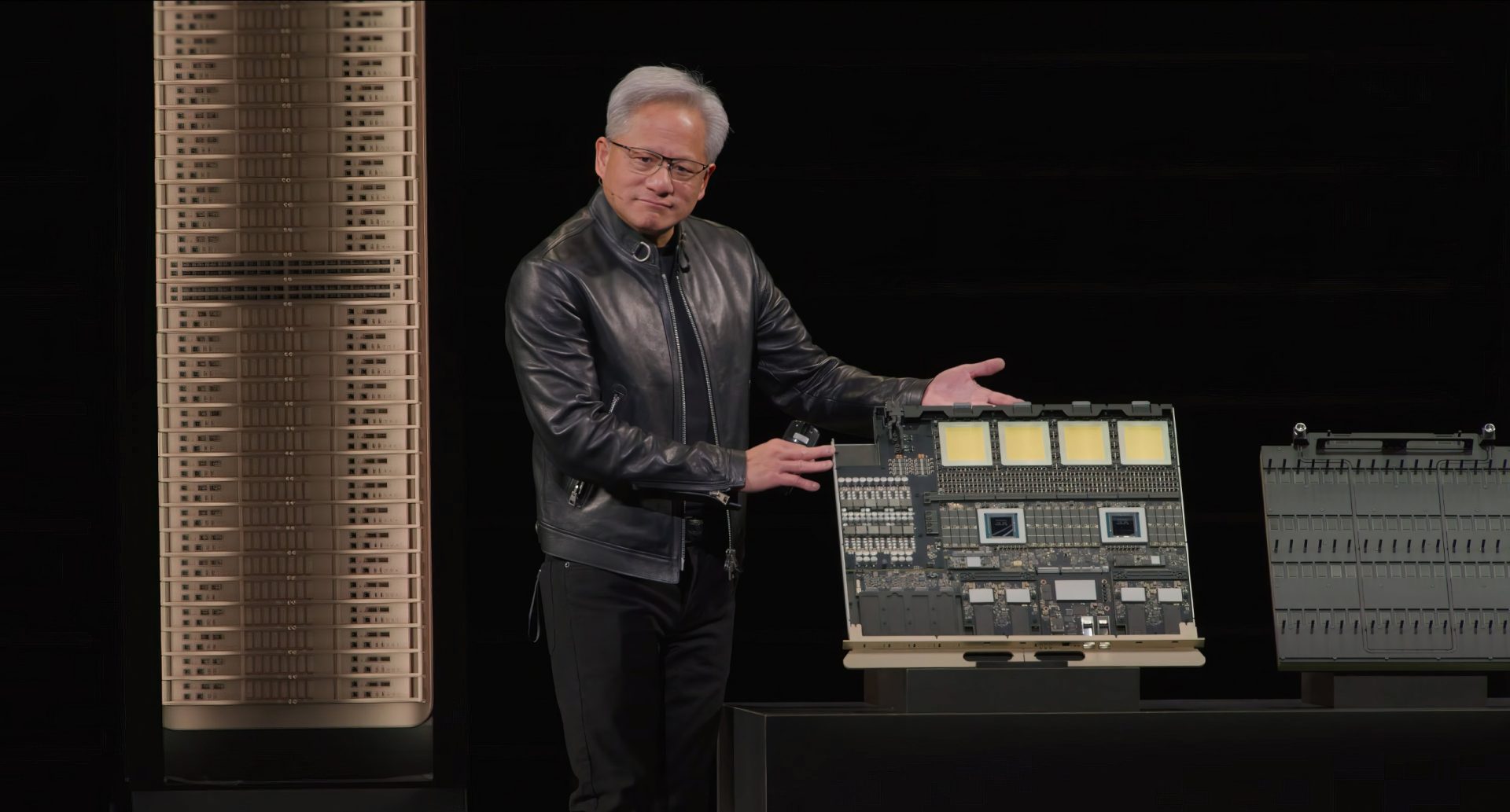
A shift from quad-chiplet to dual-chiplet design
Another major rumored change involves the Rubin Ultra compute package itself. Instead of a four-die per GPU approach, Rubin Ultra may be shifting to a two-die per GPU design. The reasoning cited is familiar to anyone watching advanced packaging: yields and warpage can become brutal when you push extremely dense multi-chip packages at scale.
Rubin Ultra is expected to rely on advanced packaging technology in the CoWoS family, where mechanical stability and manufacturing consistency become just as important as raw performance. Reducing die count can improve manufacturability, but it also threatens peak compute density—unless the system-level design makes up the difference.
To preserve performance targets, NVIDIA is rumored to be leaning on board-level assembly changes. The idea described is a 2+2 arrangement, with four Rubin Ultra GPUs housed per server node in a Kyber platform configuration. Observers also point out that prototypes shown publicly have hinted at more compact, squarer GPU modules—consistent with a two-die layout and an eight-HBM-site configuration.
Heat spreader redesigns and power-related adjustments
Late-stage thermal and mechanical tweaks are also reportedly in play. One rumor claims the heat spreader design is being updated, and that this change has contributed to delays versus earlier manufacturing expectations. Specifically, the platform may have moved from a dual heat spreader concept to a single heat spreader approach after the original design allegedly struggled to meet warpage requirements at high-volume production readiness.
On top of that, standard Rubin GPUs are rumored to be dealing with stability issues tied to the current indium-graphite thermal interface material (TIM), pushing a switch back to more traditional graphite TIM for the planned 2300W and 1800W platform variants.
A timeline circulating alongside these claims suggests Rubin Ultra could see qualification samples in July, production samples in August, mass production in September, and rack-level readiness by October—though timelines like these often shift as validation and supply chain realities collide.
Why this matters: Rubin Ultra vs AMD MI500 and the HBM4E battle
The bigger story is what these stumbles could mean for the competitive landscape in AI accelerators. Rubin Ultra and AMD’s MI500 are widely viewed as direct rivals for next-generation training and inference deployments. Both are expected to embrace major platform shifts, including co-packaged optics (silicon photonics) and advanced 2.5D/3D packaging strategies aimed at scaling bandwidth, reducing bottlenecks, and improving rack-level efficiency.
Current expectations place AMD’s MI500 launch around the second half of 2027, featuring a four-die layout and 12‑Hi HBM4E. If Rubin Ultra is truly being scaled back to a two-die package while also landing in the 2027–2028 range, AMD could have a rare chance to arrive with a more aggressive multi-die configuration at a critical moment in the HBM4E transition.
Still, it’s worth noting that NVIDIA has a track record of absorbing late-cycle design disruptions and shipping on schedule. Previous generations have faced both chip and rack-level adjustments without ultimately missing major volume production goals, and performance typically ends up close to what was originally promised.
For now, the most realistic expectation is that Rubin and Rubin Ultra issues will be mitigated as partners address yield, packaging, and thermal constraints. But the takeaway is clear: the move to HBM4 and HBM4E is not just a memory upgrade—it’s a full-platform engineering challenge. And with AMD and others pushing hard, the race to dominate AI hardware in 2027 is looking more competitive by the day.