Intel is putting its most ambitious chip packaging and manufacturing ideas on display, revealing a multi-chiplet concept that combines next-generation 18A and 14A/14A-E silicon with advanced 3D stacking and high-bandwidth interconnects. The goal is clear: enable massive, highly scalable processors built for AI, HPC, and data center workloads—while giving external customers a compelling alternative to other leading advanced packaging platforms.
At the center of Intel’s showcase is an advanced packaging approach designed to break past traditional size limits and memory constraints. Intel positions these technologies as foundational building blocks for future compute “powerhouses,” especially as demand surges for large AI accelerators and memory-rich data center processors that can scale beyond standard reticle boundaries.
Key technologies Intel highlighted include:
Intel 14A-E, featuring RibbonFET 2 and PowerDirect, aimed at delivering a major leap in logic technology.
Intel 18A-PT, described as a first “base die” with backside power for improved logic density and power delivery reliability.
High-performance top dies built on Intel 14A/14A-E, targeting better density and performance per watt for the main compute layers.
Foveros Direct 3D, using hybrid bonding at extremely fine pitch for precision 3D stacking.
EMIB-T, an evolution of EMIB that adds TSVs to boost bandwidth and enable larger multi-tile integration.
Broad HBM protocol support, covering current and future standards including HBM4, HBM5, and beyond.
More than 12x reticle scalability, enabling designs that exceed conventional packaging and manufacturing size limits.
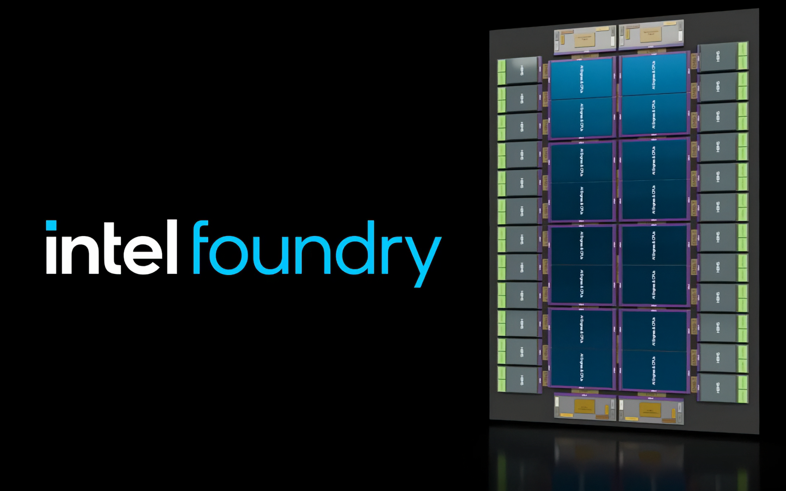
Intel’s video demonstration focuses on two conceptual packages that illustrate how far this architecture can scale. One design features four compute tiles paired with 12 HBM sites. The larger concept scales all the way to 16 compute tiles alongside 24 HBM sites, suggesting a path toward extremely large AI and HPC processors where chiplets, memory, and interconnect are engineered as one unified system.
Another striking detail is memory controller capacity. The larger concept is shown with up to 48 LPDDR5X controllers—twice as many as the smaller design—pointing to an emphasis on flexible memory configurations and higher overall memory density. That combination of HBM sites plus extensive LPDDR5X controller availability signals a platform built to serve a wide range of AI and data center needs, from bandwidth-heavy training to deployment scenarios that benefit from large memory pools.
How the stack is built: 18A-PT base die with 14A compute on top
Intel’s concept uses a compute base die fabricated on Intel 18A-PT. This base layer is presented as the foundation that can house SRAM—an approach reminiscent of how Intel has built cache-heavy designs in recent server-class architectures. Intel’s emphasis on “base die + top die” stacking suggests it wants to keep dense SRAM and critical support logic on a dedicated layer, then stack the main compute die above it for performance and scalability.
Sitting on top of that base die is the primary compute tile layer, which could include CPUs, AI engines, or other specialized IP blocks depending on the customer’s needs. Intel indicates these top compute tiles would use the Intel 14A or 14A-E process technologies, and they connect to the base die using Foveros 3D to form a high-density 3D stack.
To tie everything together across multiple tiles and out to memory, Intel uses EMIB-T. This interconnect approach is crucial for a chiplet era where performance depends not only on fast compute, but also on how efficiently tiles communicate with each other and with large pools of high-bandwidth memory. In the concept, the 24 HBM sites can support today’s HBM standards like HBM3/HBM3E as well as upcoming options such as HBM4/HBM4E and HBM5.
Why this matters for the foundry business and third-party customers
Beyond the engineering spectacle, this preview reads like a message to external customers evaluating manufacturing and packaging partners. Intel has already indicated that 18A is largely geared toward its own products, while 14A is designed with third-party adoption in mind. By showcasing a packaging roadmap that pairs 14A compute tiles with scalable 3D stacking (Foveros Direct) and a high-bandwidth bridge (EMIB-T), Intel is effectively saying it can deliver not just leading-edge nodes, but the full multi-chiplet platform needed for modern AI accelerators and data center processors.
Intel also notes it’s building a broad ecosystem and engaging with industry partners to shorten time-to-market and strengthen supply chain resilience—an increasingly important selling point as AI infrastructure demand ramps up globally.
The remaining question: when do real products arrive?
As impressive as these concepts look, the biggest test is execution. Intel has proven it can push boundaries in advanced packaging before, but ambitious multi-tile projects have also faced yield and schedule challenges in the past. Now, the industry will be watching for concrete product announcements, confirmed customers, and shipping silicon that demonstrates these packaging and node advances at scale.
Intel is positioning upcoming AI-oriented platforms as part of its comeback story, but the real make-or-break moment will be whether it can secure major third-party deals tied to Intel 14A and consistently deliver on the promise of high-scale chiplet designs. If it can, Intel’s mix of 18A/14A process technology, Foveros 3D stacking, and EMIB-T interconnect could become a serious force in next-generation AI and data center chips.