TSMC and Sony Semiconductor Solutions are teaming up to push the next wave of camera technology forward, with a new joint venture aimed at building next-generation AI image sensors. The two companies signed a non-binding memorandum of understanding on May 8, signaling serious intent to collaborate on sensors designed to “think” faster and see more intelligently than today’s camera hardware.
The planned joint venture will focus on developing and manufacturing AI-powered image sensors for some of the fastest-growing markets in imaging. That includes automotive systems such as advanced driver assistance and in-car vision, robotics applications that rely on real-time visual recognition, and advanced smartphone cameras where demand for sharper, smarter photography continues to rise.
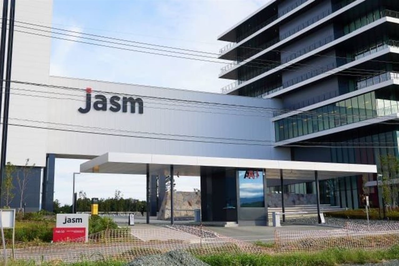
One key detail that stands out is where this project will be based. The venture is expected to be headquartered at Sony’s new facility in Kōshi, located in Kumamoto Prefecture, Japan. Kumamoto has been increasingly important in the semiconductor supply chain, and placing operations at a dedicated Sony site suggests the partnership is designed for long-term production and scaling, not just research.
Sony is also set to take the lead. Under the current plan, Sony will hold a majority stake in the joint venture and maintain operational control. That arrangement positions Sony to steer product direction and sensor design strategy, while leveraging the manufacturing expertise and semiconductor process strengths TSMC is known for.
While the agreement is currently non-binding, the announcement highlights a clear industry trend: AI image sensors are becoming central to how machines and mobile devices interpret the world. From safer cars to smarter robots and more capable smartphone cameras, this collaboration is aimed squarely at the technologies expected to define the next era of computer vision and imaging.