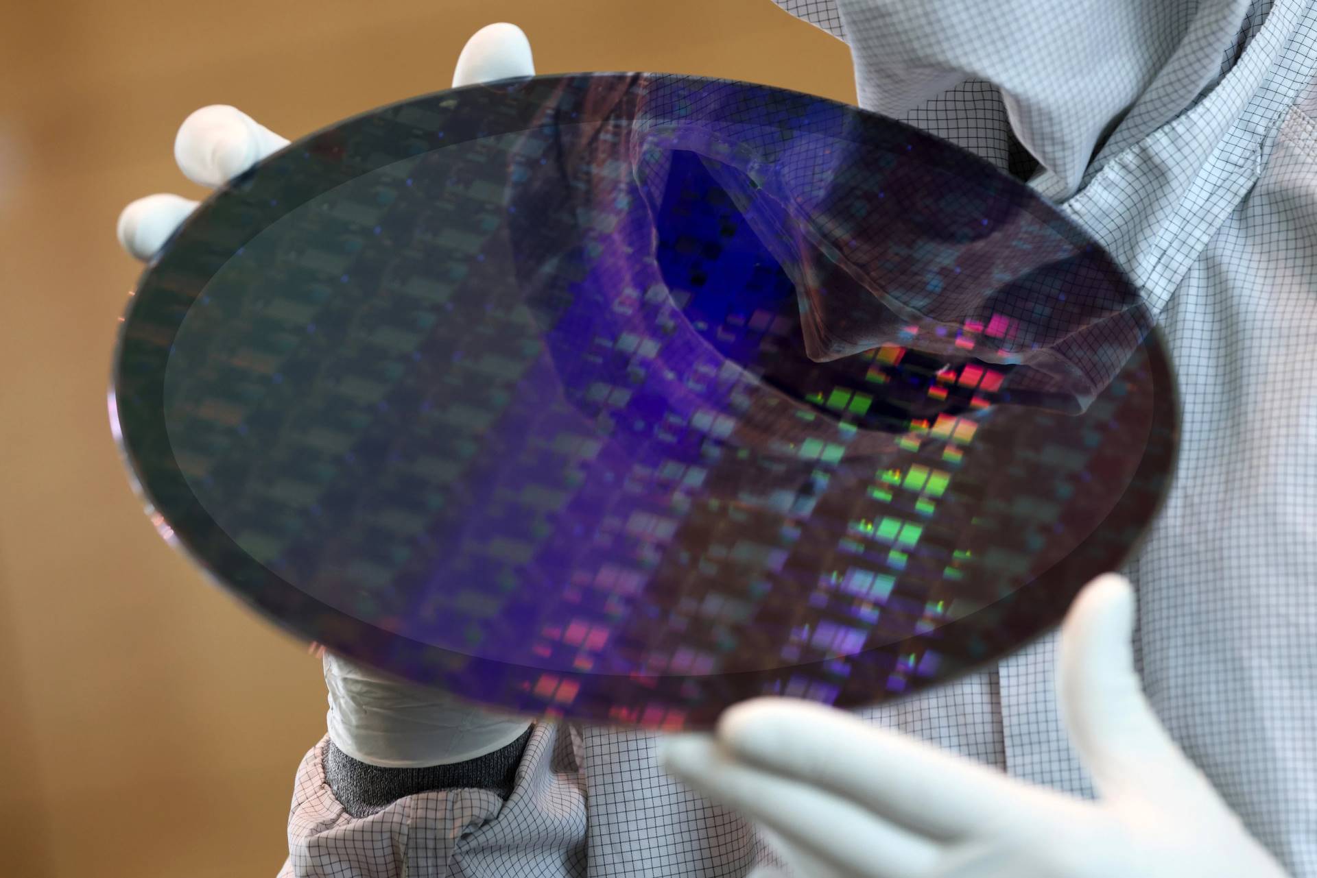
TSMC’s next-generation N2 process is shaping up to be a blockbuster. Industry chatter now points to fifteen customers already designing on the 2nm node, with around ten focused on high-performance computing. That mix signals a major shift: AI and data center silicon are set to consume a larger share of cutting-edge capacity than ever before.
The detail comes via remarks from Bren Higgins, Executive VP and CFO at KLA Corporation, who noted robust design activity at N2 and demanding performance targets from compute-focused clients. While specific names weren’t disclosed, the direction is clear. Custom AI chips from hyperscalers and ASIC vendors are expected to be a big part of the early 2nm ramp, with companies like Google, Broadcom, Amazon, and even OpenAI widely reported to be developing in-house accelerators. Add in next-gen platforms from NVIDIA and AMD—such as NVIDIA’s Rubin Ultra and AMD’s Instinct MI450—and it’s easy to see why HPC is poised to dominate initial adoption.
Mobile will still matter. Historically, early nodes have leaned on smartphone leaders to drive volume, and that pattern should continue with Apple, MediaTek, and Qualcomm among the first wave of adopters. But the balance is changing. AI training, inference, and data center workloads are setting the pace for performance and energy efficiency at the bleeding edge, and those priorities will heavily influence how N2 matures.
Another reason momentum is building: pricing. Reports suggest TSMC’s 2nm offering is structured to be more attractive than the preceding 3nm generation, helping to unlock broader uptake—especially among HPC customers who are racing to pack more compute into tighter power budgets. As a result, overall 2nm output is expected to outstrip 3nm, reflecting both stronger demand and a wider range of high-value applications.
On timing, mass production for N2 is currently targeted for the second half of 2026, setting the stage for the first major wave of launches in early 2027. With design work already underway, expect aggressive product roadmaps and rapid iteration as the ecosystem pushes to capitalize on 2nm’s performance-per-watt gains.
Bottom line: TSMC’s 2nm node won’t just be another process shrink. It’s arriving at the heart of the AI boom, with HPC, custom silicon, and mobile all converging to create one of the most consequential manufacturing ramps in recent memory.