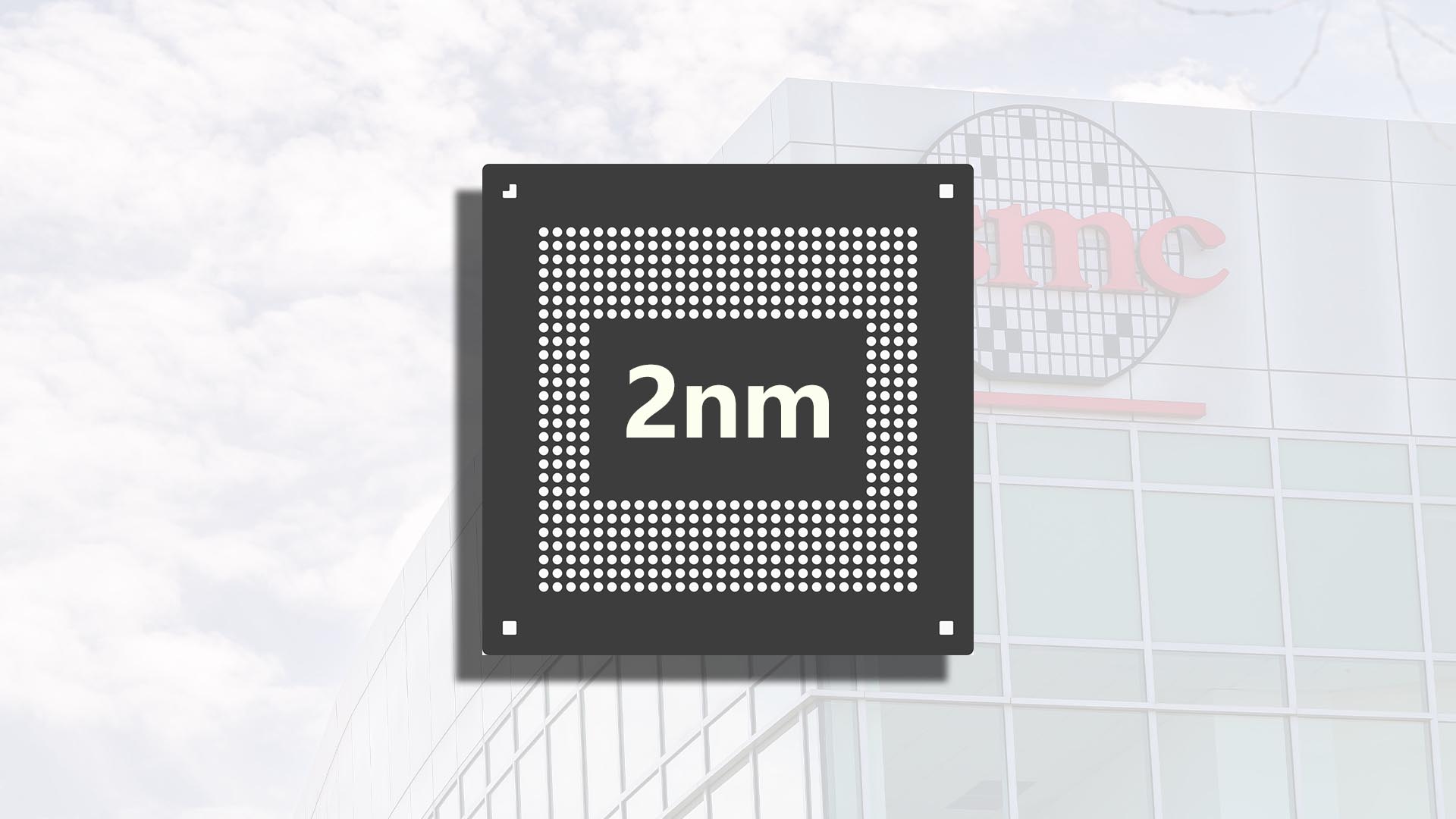
TSMC’s first 2nm chips are expected to arrive in 2026, and early chatter has painted them as potentially expensive, with some estimates putting 2nm wafer pricing around $30,000. That kind of number instantly raises concerns for phone makers and chip designers planning next-generation launches. Now, a new rumor suggests those sky-high pricing claims may be exaggerated, offering a more encouraging outlook for the companies lining up to use TSMC’s 2nm technology.
According to a Weibo tipster known as Smart Chip Insider, multiple 2nm chip projects are progressing smoothly and remain on track for 2026. While the post doesn’t name specific brands, it does claim two important things: first, that the power, performance, and area improvements of TSMC’s 2nm N2 node may be more limited than some people expect; and second, that 2nm wafers won’t be priced at an “outrageous” level.
If that proves accurate, it could be a relief for major mobile chip players, especially as other component costs are also rising. Smartphone processors don’t exist in a vacuum, and memory pricing has been a growing concern. With tighter margins across the industry, saving even a little on wafer costs can meaningfully impact the final bill of materials for flagship devices.
On the product side, the first wave of 2nm smartphone chipsets is already taking shape. Apple is widely expected to be first to market with its A20 and A20 Pro, produced on TSMC’s 2nm process. Not far behind, Qualcomm’s next generation Snapdragon 8 Elite Gen 6 and Snapdragon 8 Elite Gen 6 Pro are anticipated to follow, with MediaTek’s Dimensity 9600 also tipped to enter the 2nm era.
Memory strategy is becoming part of the bigger 2026 performance-and-cost equation. A separate leak previously suggested Qualcomm and MediaTek may push for LPDDR6-only support on their upcoming flagship chips, driven by ongoing memory cost increases. Interestingly, rather than using the base 2nm N2 node, both companies are also rumored to choose the more advanced 2nm N2P variant. The catch is that the reported performance gain from N2 to N2P is relatively small, around 5 percent, which underscores how incremental these node upgrades may be at the leading edge.
That lines up with broader expectations around TSMC’s 2nm N2 capabilities. The N2 node is said to deliver about a 15 percent performance improvement over TSMC’s 3nm N3E, along with up to a 30 percent reduction in power. Those are meaningful gains in isolation, especially for battery life and sustained performance. However, if you’re comparing newer 3nm variants like N3P to 2nm N2, the real-world jump could feel less dramatic, reinforcing the claim that PPA improvements may not be huge for every customer use case.
Even modest progress still matters in flagship smartphones, where every efficiency gain can translate into cooler devices, longer battery life, and more headroom for AI features and advanced camera processing. The bigger question for 2026 will be how companies balance these incremental improvements against manufacturing costs, memory pricing, and competitive pressure.
For now, the most notable takeaway is simple: despite earlier sticker-shock projections, 2nm wafers may not be as wildly expensive as feared. If pricing ends up more reasonable, it could help Apple, Qualcomm, MediaTek, and others bring 2nm-powered phones to market without pushing flagship prices even higher.