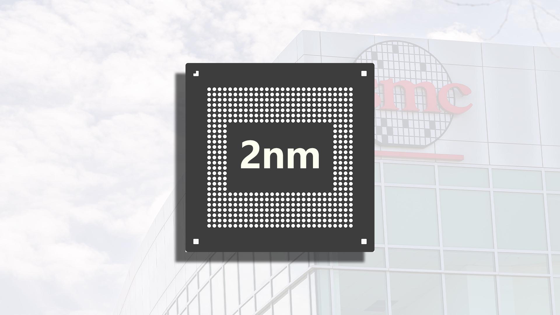
TSMC’s next big node is almost here. The chipmaker is preparing to kick off 2nm mass production in the fourth quarter of 2025, setting the stage for a broader industry shift to the N2 process in 2026. According to industry reports, Apple has already locked down nearly half of the initial capacity, positioning the A20 and A20 Pro chips for the iPhone 18 lineup as early showcases for the new node.
TSMC began taking 2nm orders on April 1 with an initial target of roughly 50,000 wafers per month by the end of 2025. The company is aiming to double down in 2026, with monthly output expected to reach around 100,000 wafers. Longer term, capacity should expand further as the Arizona fabrication plant comes online to support the node, helping push total 2nm output toward 200,000 wafers per month by 2028.
Pricing and customers paint a clear picture of demand at the cutting edge. Each 2nm wafer is expected to cost about $30,000, yet interest remains intense. Apple and Qualcomm are poised to be among the largest early buyers, with AMD, MediaTek, Broadcom, and others in the queue. TSMC’s trial production earlier this year reportedly achieved yields around 60%, and the rate is said to be improving as more capacity spins up across facilities in Taiwan.
Most 2nm wafer starts will be concentrated at TSMC’s Baoshan and Kaohsiung plants, while 3nm and 4nm lines remain fully booked throughout 2026—another sign that demand across nodes remains exceptionally strong. Expect some 2nm tape-outs to begin as early as the fourth quarter, with MediaTek publicly signaling its intent to move quickly in a bid to get ahead of rivals.
What this means for devices and the market:
– Earlier access for Apple suggests iPhone 18 models could headline the first wave of 2nm-powered smartphones via A20 and A20 Pro chips.
– Qualcomm’s participation points to next-gen Snapdragon platforms pivoting to 2nm soon after, with ripple effects across Android flagships.
– MediaTek’s accelerated tape-out plans could translate into Dimensity-branded 2nm chips aimed at premium and upper-midrange devices.
– The steep $30,000-per-wafer cost raises the odds that some of these expenses will be passed through to end products, potentially nudging flagship prices higher.
Why 2nm matters: TSMC’s N2 node introduces a new transistor architecture generation that is expected to deliver sizable gains in performance and power efficiency versus 3nm-class processes. For consumers, that typically translates into faster chips, longer battery life, thinner devices, or some mix of all three. For chip designers, the combination of higher density and efficiency makes N2 a prime target for mobile processors, AI accelerators, and power-sensitive computing.
Key timelines to watch:
– Q4 2025: Start of 2nm mass production; first customers ramping
– 2026: Capacity scaling toward 100,000 wafers per month; broad industry transition begins
– 2028: Output expected to approach 200,000 wafers per month with support from the Arizona fab
All signs point to a fierce race for early 2nm capacity. With Apple securing a large initial share and other heavyweights lining up, the next year will be critical for tape-outs, yield improvements, and pricing strategy—factors that will shape the performance and price tags of 2026’s most advanced devices.


