Elon Musk has offered the first official glimpse of Tesla’s next in-house AI processor, the Tesla A15 chip, confirming that it has successfully reached “tape-out” and sharing early images of the package. The update signals a major milestone for Tesla’s autonomous driving hardware roadmap, and it also comes with a clear message: A15 is only the beginning, with A16 and Dojo3 already in development.
In Musk’s post on X, he congratulated Tesla’s AI team and thanked both TSMC and Samsung for helping bring the chip to production. He also suggested the A15 could become one of the most widely produced AI chips ever, reflecting Tesla’s potential scale once the chip moves into high-volume manufacturing.
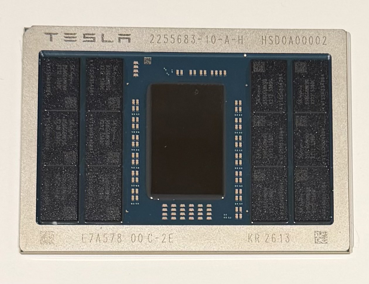
The images Musk shared show a design centered around a large primary compute die, surrounded by 12 memory modules. This layout points to a high-bandwidth, efficiency-focused approach—an important factor for real-time AI workloads like Full Self-Driving (FSD). The memory modules visible in the photo appear to be from SK hynix, and the markings indicate the chip was taped out during the 13th week of 2026 (roughly March 23–29).
A15 is positioned as the successor to Tesla’s HW4 platform and is expected to power the company’s next-generation FSD solution. Musk has previously described A15 as a dramatic leap forward compared to HW4, claiming up to a 40x improvement overall, including roughly 8x gains in raw compute performance and 9x more memory, along with support for new capabilities. The chip is said to be designed with modern transformer-style AI processing in mind, aligning with where the broader AI industry is headed.
On the performance side, the A15 has been associated with figures around 2500 TOPS of AI compute and up to 144 GB of memory per chip. While Tesla hasn’t published a full specification sheet, the stated goals suggest a platform built not just for incremental driving improvements, but for a much heavier on-device AI workload and faster iteration on new autonomy features.
Musk has also emphasized how critical the chip is to Tesla’s strategy, previously calling the effort to “solve” A15 an existential task for the company. He described spending months working on it personally on Saturdays, underscoring how central custom silicon has become to Tesla’s autonomy plans.
Interestingly, Tesla appears to be targeting multiple A15 configurations. One version is described as a single-SoC design intended to compete with high-end data center class AI capability, and another as a dual-SoC approach aiming even higher—while prioritizing lower cost and lower power consumption. If Tesla can deliver on those efficiency and cost claims at scale, A15 could become a key differentiator for the company’s vehicle AI stack.
Manufacturing is expected to involve both TSMC and Samsung, with high-volume production targeted for late 2026 or early 2027. Musk has also mentioned a longer-term plan to shift next-generation chip production to Tesla’s upcoming “TeraFab,” though formal details and a full announcement have yet to appear.
Beyond A15, Musk confirmed that development is already underway for the Tesla A16 chip as well as Dojo3, the next stage of Tesla’s AI training and supercomputing ambitions. Tesla revived its supercomputer project plans earlier in 2026, and the company’s push toward tighter vertical integration—bringing memory, packaging, and chip development closer together—suggests Tesla wants faster development cycles and more control over both training and inference hardware.
For anyone tracking Tesla Full Self-Driving progress, AI compute trends, or the race to build more efficient AI chips, A15’s tape-out is a major signpost. It marks the transition from bold claims to real silicon—and sets the stage for the next wave of Tesla autonomy hardware in the years ahead.