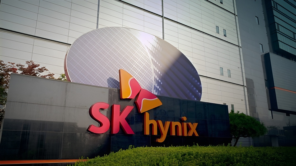
SK hynix, one of the world’s leading memory makers, is preparing a major expansion in South Korea as demand for AI-focused memory continues to surge. The company has announced plans to build new advanced packaging production lines in Cheongju, a move designed to ease a growing pressure point in the AI hardware supply chain.
Advanced packaging has quickly become a critical bottleneck for the AI industry. As AI chips grow more complex, many designs increasingly rely on packaging technologies that bring high-bandwidth memory (HBM) closer to the main compute chip to boost speed and efficiency. For major AI platforms, the ability to tightly integrate HBM with the compute die is no longer a nice-to-have feature; it’s essential. That’s why expanding advanced packaging capacity is becoming just as important as producing the memory itself.
To address this, SK hynix plans to invest up to about $13 billion in a new advanced packaging facility known as P&T7. The goal is to strengthen the company’s ability to respond consistently to global AI memory demand while improving production efficiency at its Cheongju operations. SK hynix also framed the decision as aligning with broader policy goals around balanced regional growth, while keeping a close eye on supply chain performance and long-term competitiveness.
A key detail is how this new facility fits into SK hynix’s broader manufacturing roadmap. P&T7 is positioned to work in tandem with the company’s upcoming M15X DRAM fab, creating what SK hynix describes as an “organic linkage” between the sites. In practical terms, this could allow SK hynix to offer a more streamlined, end-to-end path for customers: DRAM and HBM-related components can be produced and then moved directly into advanced packaging lines nearby for stacking and final processing. The company is aiming to create a one-stop solution for HBM customers within the Cheongju Techno Valley Industrial Complex.
This investment also highlights a bigger competitive question in the AI semiconductor race: who controls the most advanced packaging capacity, and who can scale it fastest? While SK hynix already uses MR-MUF vertical stacking for its HBM products, packaging at the full chip level has often depended on external partners. By building out more advanced packaging infrastructure, SK hynix appears to be positioning itself to deliver a more complete turnkey offering for AI customers and to strengthen its standing in the fast-growing HBM market.
SK hynix has not yet shared which specific advanced packaging technologies P&T7 will prioritize. That leaves open several possibilities, including partnerships with established packaging specialists or deeper collaboration through investment to bring advanced packaging output into SK hynix-controlled facilities. Another potential path is the development of a proprietary approach that would reduce reliance on outside foundry and packaging ecosystems over time.
With AI demand continuing to reshape the semiconductor industry, SK hynix’s push into expanded advanced packaging capacity signals how seriously the company is taking the next phase of the AI memory boom. By building the manufacturing and packaging pipeline closer together, SK hynix is aiming to deliver faster, more scalable supply for customers who can’t afford delays in the race to deploy more powerful AI hardware.