SK Hynix Pushes to Open Yongin Triple-Deck Chip Fab by 2027 as AI Memory Demand Soars
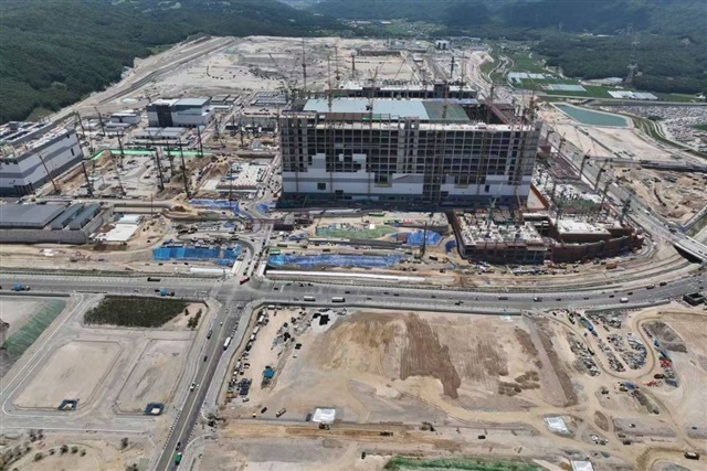
SK Hynix is moving fast to bring its next major semiconductor production site online, with plans to complete the first cleanroom at the Yongin Semiconductor Cluster in Gyeonggi Province, South Korea, by February 2027. The accelerated timeline highlights how urgently the company is preparing for the next wave of demand in advanced memory chips, especially as artificial intelligence continues to reshape the global semiconductor market.
The Yongin Semiconductor Cluster is one of South Korea’s most ambitious chip manufacturing projects. Once fully developed, the site is expected to become a key production hub for SK Hynix, supporting the company’s long-term expansion in DRAM, high-bandwidth memory, and other advanced semiconductor technologies.
What makes the first fab especially notable is its planned triple-deck structure. Instead of following the more traditional single-level cleanroom design used in many fabrication plants, the facility is expected to use a stacked layout that allows more production space within a limited footprint. This approach could help SK Hynix improve efficiency, speed up future expansion, and better handle the enormous infrastructure demands of next-generation chip manufacturing.
The race to finish the first cleanroom by early 2027 comes at a crucial time for the memory industry. Demand for high-performance memory has surged due to the rapid growth of AI servers, data centers, graphics processors, and cloud computing systems. High-bandwidth memory, often referred to as HBM, has become particularly important because it enables faster data transfer and greater energy efficiency for AI accelerators.
SK Hynix has already established itself as a major supplier in the HBM market, and the Yongin site could strengthen its position even further. As AI companies and data center operators look for more powerful hardware, chipmakers are under pressure to secure enough manufacturing capacity to meet future demand. The faster SK Hynix can bring new production lines online, the better positioned it will be in the global memory race.
The Yongin project also reflects South Korea’s broader strategy to maintain its leadership in advanced semiconductors. The region is being developed as a large-scale chip ecosystem, combining manufacturing facilities, suppliers, research operations, and supporting infrastructure. For SK Hynix, the cluster is not just another fab site; it is a long-term foundation for competing in one of the world’s most important technology sectors.
Building a cutting-edge semiconductor plant is an extremely complex process. Cleanrooms must meet strict standards for air purity, vibration control, temperature stability, and contamination prevention. Even tiny particles can affect chip yields, making cleanroom construction one of the most critical stages in fab development. Completing the first cleanroom by February 2027 would mark a major milestone for the Yongin facility and could pave the way for equipment installation and future production ramp-up.
The triple-deck design may also offer strategic advantages. By stacking cleanroom space vertically, SK Hynix can potentially increase production density while reducing the need for a wider building footprint. This could be especially valuable in a mega-cluster environment where infrastructure planning, utilities, and logistics all need to be carefully coordinated.
Although the semiconductor industry is known for cycles of boom and slowdown, the long-term outlook for AI memory remains strong. Training and running advanced AI models requires massive computing power, and that computing power depends heavily on fast, efficient memory. As a result, companies that can supply high-end memory at scale are likely to play a central role in the next phase of AI infrastructure growth.
SK Hynix’s push to accelerate the Yongin fab shows that the company is preparing for that future now. If the cleanroom is completed on schedule in 2027, the site could become one of the most important additions to the global memory supply chain.
With its massive scale, advanced design, and focus on next-generation chip production, the Yongin Semiconductor Cluster is shaping up to be a major piece of SK Hynix’s growth strategy. As competition intensifies in AI memory and high-performance computing, the company’s ability to execute this project quickly could become a decisive advantage.