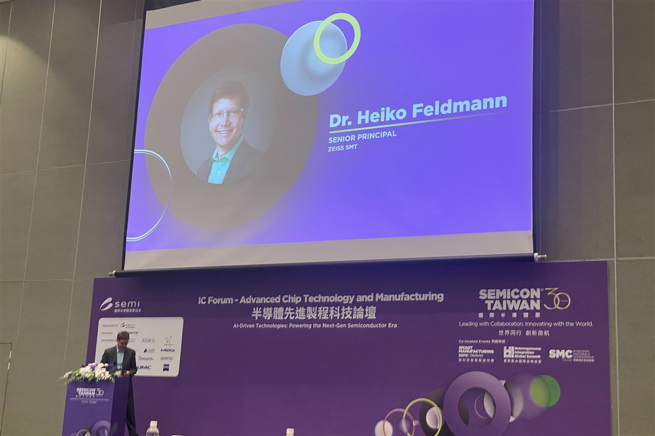
Zeiss maps the next leap in chipmaking: from High NA to Hyper NA EUV at SEMICON Taiwan 2025
Zeiss Semiconductor Manufacturing Technology used the stage at SEMICON Taiwan 2025 to lift the curtain on where advanced lithography is headed next. In a rare look ahead, the company outlined its optics roadmap, charting a path from the current era of High NA EUV to the next frontier: Hyper NA. It’s a signal that the industry’s push for finer features, higher performance, and better power efficiency is set to accelerate.
EUV lithography has already transformed how the most advanced chips are made. The jump to High NA boosted resolution by capturing light at steeper angles, allowing tighter patterning and more precise features on silicon. Hyper NA takes that concept even further. By increasing the numerical aperture again, it aims to resolve even smaller details, expanding what’s possible for cutting-edge logic, memory, and heterogeneous integration.
Why this matters
– More computing in less space: Higher resolution enables denser transistor layouts and more complex designs without ballooning die size.
– Better performance per watt: Tighter pattern control can translate into faster chips that consume less energy.
– Longer runway for innovation: Extending EUV’s capability helps keep advanced nodes on track for applications spanning AI, data centers, mobile devices, automotive, and beyond.
What Hyper NA could demand
– Next-level optics: Even more exacting mirrors and optical assemblies to manage extreme precision at higher angles.
– Materials and resist advances: Chemistry tuned for finer features and improved line-edge roughness.
– Mask and metrology evolution: Sharper inspection, defect control, and calibration to sustain yield at smaller geometries.
– Ecosystem readiness: Coordinated progress across toolmakers, materials suppliers, and fabs to bring new platforms into high-volume manufacturing.
The roadmap from High NA to Hyper NA suggests a deliberate, stepwise progression—refining optical performance, process control, and manufacturability along the way. It underscores how crucial optics are to the future of semiconductor scaling and how collaboration across the supply chain will be essential to turn Hyper NA from ambition into production reality.
Bottom line: By outlining a clear optics trajectory at SEMICON Taiwan 2025, Zeiss is signaling confidence in the next phase of EUV lithography. High NA is the present. Hyper NA is the horizon. And the industry now has a sharper view of how it plans to get there.
 and A12 (1.2nm) for 2029, Holding Off on ASML’s Most Expensive EUV Machines—for Now")


