Samsung’s 2 nm chip program is moving from promise to execution, with fresh data showing steady gains in performance, power efficiency, and—most importantly—yield. The update suggests the company is on a credible path to mass production and a more competitive position at the leading edge of semiconductor manufacturing.
Here’s what’s new. Samsung’s 2 nm Gate-All-Around (GAA) node now delivers a 5% performance uplift and an 8% boost in power efficiency versus its own 3 nm GAA process, while trimming chip area by 5%. The performance gains are modest, but the area reduction is meaningful. Denser layouts and improved thermals can enable more compact designs—ideal for AI accelerators and next-gen mobile processors where every milliwatt and square millimeter matters.
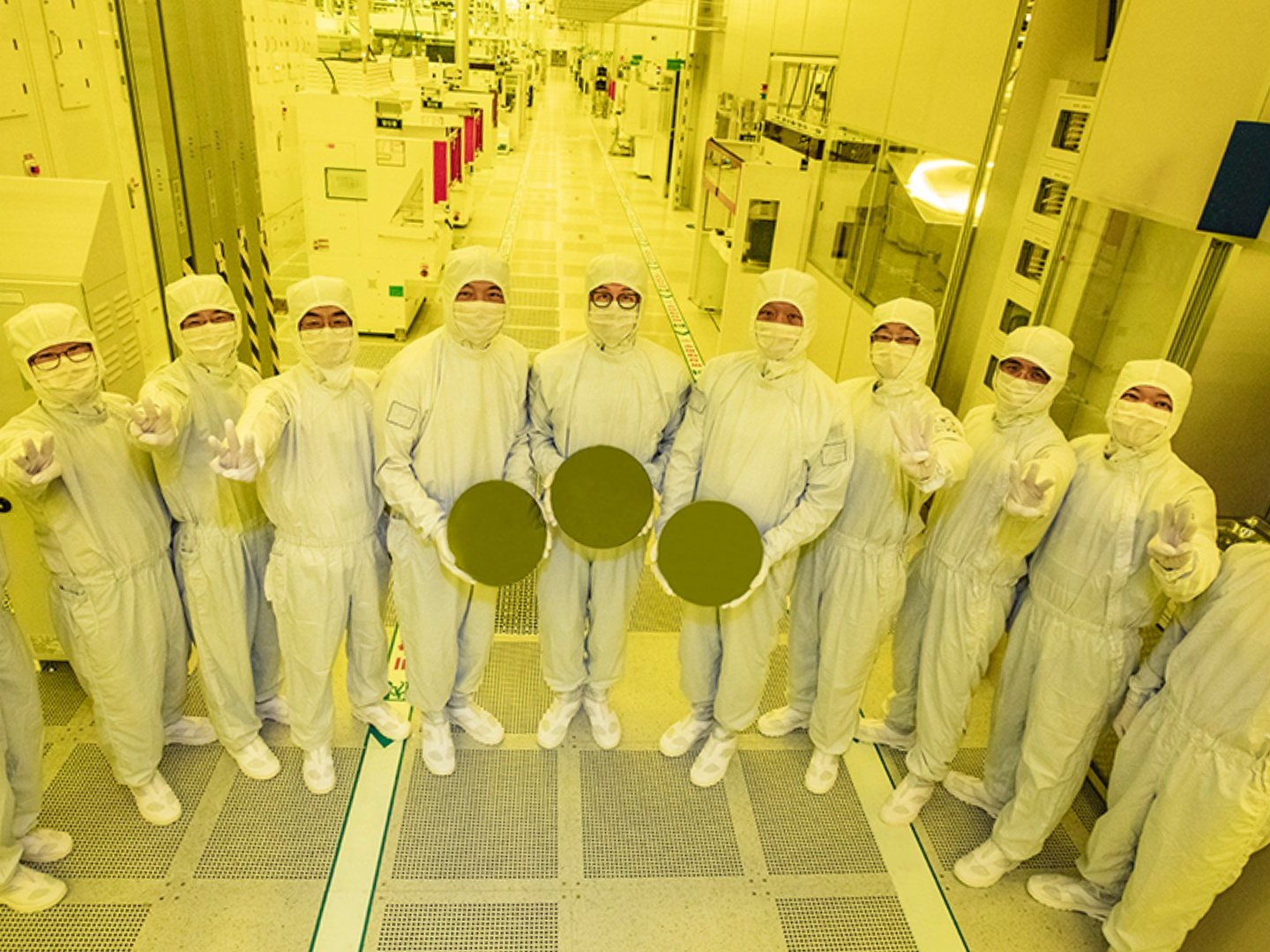
The real breakthrough is yield. Samsung says 2 nm yields have climbed into the 50–60% range, a significant jump from earlier estimates near 30%. That’s a turning point for cost, capacity, and customer confidence. Higher yields lower cost per chip, support larger wafer starts, and set the stage to ramp production for the Exynos 2600. With efficiencies improving, the chip division could return to profitability by 2027.
Commercial traction is building as well. Samsung has secured multiple 2 nm contracts with cryptocurrency mining hardware makers MicroBT and Canaan, signaling that its performance-per-watt targets are resonating in one of the most efficiency-sensitive markets. Even more impactful, a long-term agreement worth $16.5 billion with Tesla through 2033 highlights the company’s capability to support high-volume, multi-year supply in automotive and advanced compute.
Context still matters. The global foundry market is dominated by TSMC at roughly 70.2% share, with Samsung near 7.3%. Closing that gap won’t happen overnight. But rising yields, incremental node gains, and high-profile contracts together form a realistic path to greater relevance as the industry transitions to 2 nm and beyond.
Why 2 nm GAA matters
– GAA transistors improve current control and reduce leakage at high densities, boosting efficiency without sacrificing performance.
– Even small area reductions can be repurposed for larger on-die cache, more AI acceleration blocks, or additional modem and imaging features—without raising power or heat.
– Yield is the difference between lab success and profitable production. Hitting the 50–60% range marks a key milestone for scaling output.
What to watch next
– Exynos 2600 timing and real-world results: Pairing 2 nm gains with mature design tools and robust packaging could deliver noticeable battery life and thermal improvements in upcoming smartphones.
– Expansion beyond mobile: Expect 2 nm to show up in specialized compute where performance-per-watt rules, from AI-centric hardware to automotive platforms.
– Continued yield and area progress: Even incremental improvements can materially reduce cost and sharpen competitiveness at advanced nodes.
Bottom line
Samsung’s 2 nm progress isn’t about eye-popping benchmark leaps—it’s about disciplined execution. A solid efficiency bump, meaningful area savings, and a decisive yield improvement, reinforced by long-term customer commitments, indicate the company is on track to compete more seriously at the leading edge. For mobile, AI, and automotive players seeking diversified advanced-node supply, this is a development worth watching.