Samsung is mounting an aggressive comeback in the foundry business, targeting a return to profitability within the next two years and setting its sights on a 20% market share by 2027. While the market remains dominated by TSMC, Samsung is betting big on next-generation manufacturing, long-term customer partnerships, and strategic capacity expansion to close the gap.
The challenge is real. Since 2022, Samsung’s foundry division has posted quarterly losses estimated between 1 trillion won (around $0.68 billion) and 2 trillion won (around $1.36 billion). Despite significant investments in advanced nodes, orders have lagged—an issue often tied to the perception of weaker yields and reliability in past process generations. To change the narrative, Samsung has put a two-year business plan in motion, securing equipment and infrastructure in advance to ensure it can fulfill incoming demand quickly.
A core pillar of this turnaround is Samsung’s rapid progress with 2nm gate-all-around (GAA) technology. The company is prioritizing yield improvements on its first-generation 2nm GAA process while having already completed the basic design for a second-generation 2nm node. This advanced technology is slated to power the upcoming Exynos 2600, expected to appear in the base Galaxy S26 and Galaxy S26 Plus models targeted for a February launch window. The move signals confidence that Samsung’s most advanced process is ready for high-volume, consumer-grade products.
Customer momentum is another major piece of the puzzle. A reported $16.5 billion agreement with Tesla is seen as a breakthrough for Samsung’s foundry pipeline, reinforcing the company’s push into high-value, long-term contracts. In mobile chipmaking, Samsung has also provided Snapdragon 8 Elite Gen 5 samples to Qualcomm for evaluation, positioning itself as a potential manufacturing partner for next year’s Snapdragon 8 Elite Gen 6 and 8 Elite Gen 6 Pro. Securing such flagship orders would validate Samsung’s 2nm GAA platform and help shift industry sentiment in its favor.
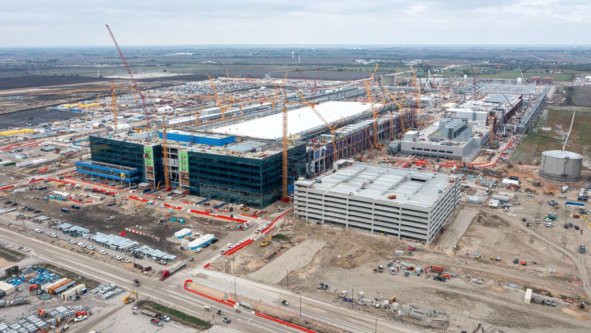
Geographic diversification and capacity readiness are equally important for the plan to work. Samsung’s Taylor, Texas facility currently produces mature process nodes ranging from 14nm to 65nm, but efforts are underway to significantly upgrade the site. ASML has reportedly formed a team to install EUV lithography equipment at the plant, preparing it for advanced-node operations slated to begin in 2026. Boosting utilization at Taylor will be critical to improving overall profitability and offering customers additional, geographically diverse capacity.
Samsung’s 2027 goal is clear: capture 20% of global foundry sales and prove that its leading-edge processes can compete at scale. To get there, the company must execute on three fronts:
– Drive 2nm GAA yields to competitive levels and accelerate the transition to its second-generation 2nm design.
– Convert high-profile evaluations into multi-year, high-volume orders across mobile, automotive, and AI-centric workloads.
– Ramp EUV-enabled capacity in Texas while maintaining stability and efficiency across its global fabs.
The stakes are high, but the strategy is cohesive. With 2nm GAA ramping, an expanding customer roster, and EUV capacity coming online in the United States, Samsung is aligning technology, operations, and partnerships to stage a credible challenge in the semiconductor foundry race. If it can sustain momentum and deliver consistent yields, the path to profitability—and a much larger slice of the market—looks within reach by 2027.