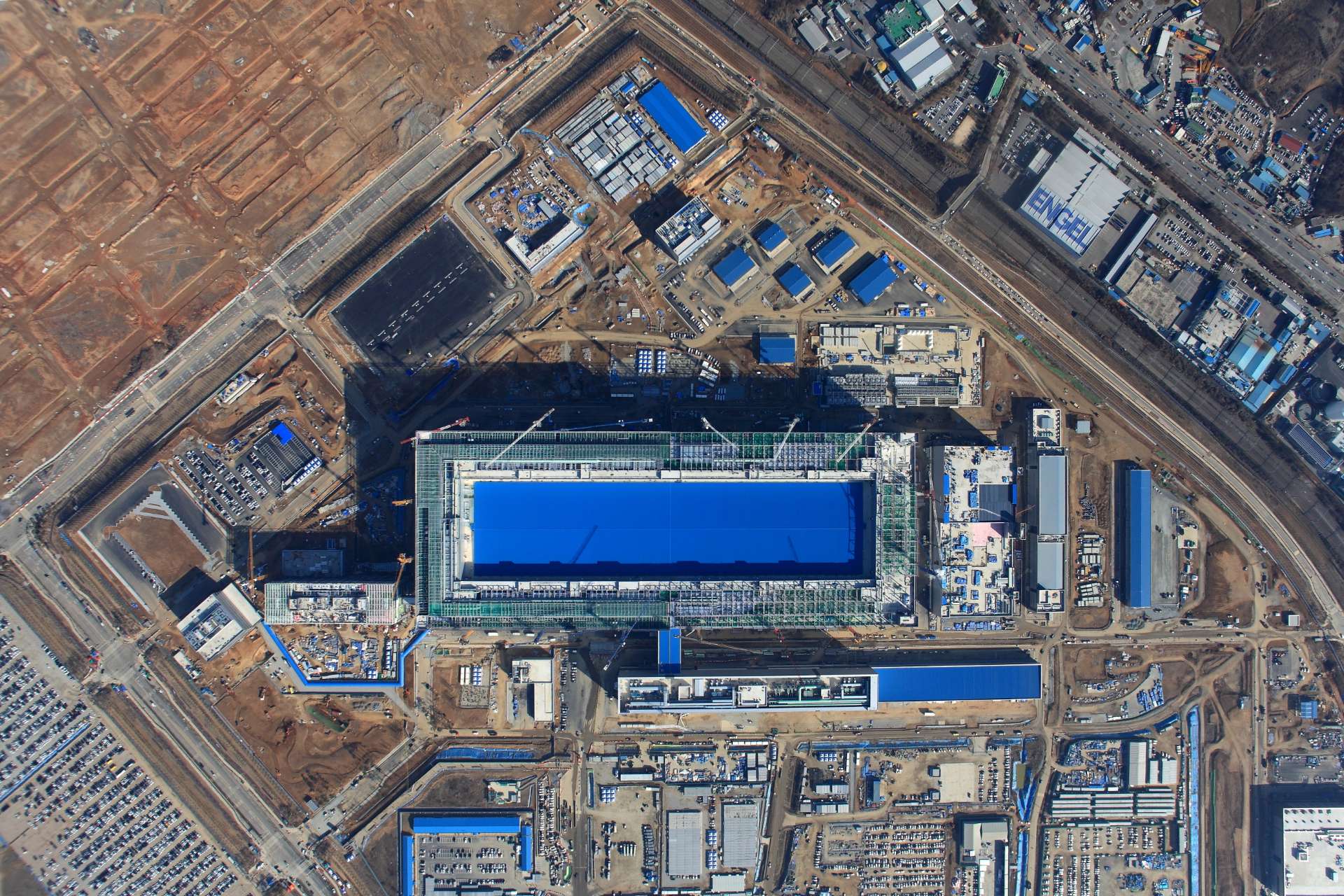
Samsung’s chip foundry business is finally showing clear signs of a turnaround after a rough stretch that saw production lines running well below capacity.
In the second half of last year, Samsung Foundry’s utilization rate reportedly hovered around 50 percent, a level that typically signals weak demand and inefficient operations. New reports now suggest that figure has climbed to around 60 percent. It’s not a full recovery yet, but it’s a meaningful step in the right direction—especially as Samsung continues chasing a bigger goal: getting its foundry division back to profitability by 2027.
A big part of the story comes down to manufacturing yields, which are critical in the semiconductor industry. Samsung’s early 3nm GAA (Gate-All-Around) process struggled with low yields, and that hurt customer confidence. When yields are poor, more chips fail testing, costs soar, and customers often shift orders to competitors with more consistent output. Those 3nm issues contributed to heavy losses, with reports indicating Samsung’s non-memory operations were in the red by roughly 2 trillion won (about $1.36 billion) at one point.
Now, there’s progress on multiple fronts. Samsung’s next-generation 2nm GAA yields are reportedly improving and sitting around 50 percent. That’s an important milestone because 2nm is a key battleground for future AI processors, smartphone chipsets, and advanced computing. Samsung has also managed to land major business, including a widely reported $16.5 billion agreement with Tesla tied to production of the AI6, along with additional chip production work linked to Chinese cryptocurrency equipment makers.
But here’s the twist: the recent boost in foundry utilization doesn’t appear to be driven primarily by 2nm demand—at least not yet. Instead, the near-term recovery is being powered by stronger orders on Samsung’s more mature nodes, especially 4nm and 8nm. That’s significant because these processes are widely used for today’s AI accelerators, mobile chips, and other high-volume products where customers want reliable output at a manageable cost.
Importantly, Samsung’s 4nm yields are said to be in a much healthier 60–70 percent range, making it far easier to deliver consistent volumes. That improved stability has reportedly helped Samsung win new business, including an order valued around $100 million from a U.S.-based AI company to develop an “Omni” processor.
Financially, the situation also looks less severe than before. The earlier deficit of about $1.36 billion was reportedly cut to around 1 trillion won (roughly $680 million) during the third and fourth quarters of 2025, a sign that the business is slowly moving toward breakeven.
Meanwhile, Samsung’s memory division is benefiting from market conditions going in the opposite direction. Ongoing shortages have strengthened memory pricing and demand, putting Samsung’s memory business in a strong position. Even so, the company appears cautious about ramping output too aggressively. Reports suggest Samsung increased DRAM production by only about 5 percent to around 8 million wafers—still below projected demand—likely to avoid oversupplying the market once demand cools.
Taken together, the picture is clearer than it’s been in a while: Samsung isn’t fully out of the woods, but better utilization, stronger 4nm/8nm traction, and improving advanced-node yields are helping the company stabilize its foundry business. If that momentum continues, Samsung’s 2027 profitability target for the foundry division looks more realistic than it did during the worst of the 3nm struggles.