Samsung boosts 1c DRAM yield near 80%, strengthening its HBM4 push as Nvidia tests loom
Samsung Electronics has raised the yield of its sixth-generation 1c DRAM to nearly 80%, a milestone that sharpens its competitiveness in next-generation HBM4 memory. With production ramping at the company’s advanced Pyeongtaek manufacturing complex and joint testing with Nvidia underway, qualification results are expected by November 2025.
Why this matters: Yield is one of the most important indicators of manufacturing maturity for cutting-edge semiconductors. Near-80% yield on a 1c node signals a healthier, more efficient process that can translate to better supply stability, improved costs, and faster time-to-market. For HBM4—designed to feed data-hungry AI accelerators and high-performance computing systems—higher yields can be the difference between a smooth rollout and constrained availability.
What 1c DRAM brings to HBM4: The 1c node, part of the sixth generation in the industry’s scaling roadmap, aims to pack more bits per area while controlling power and reliability. Consistent yields at this level can streamline stacking for HBM4, where multiple DRAM layers are integrated with a high-speed interface. That combination is essential for AI training and inference, where memory bandwidth has become as critical as compute.
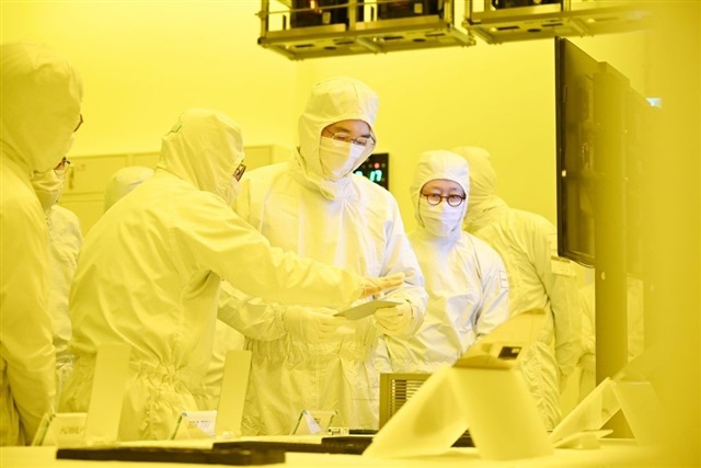
Production ramp at Pyeongtaek: The Pyeongtaek campus is one of the world’s largest memory manufacturing hubs, and a ramp there points to readiness for higher volumes once qualifications are complete. A stable ramp also helps downstream partners plan their own product timelines, whether for servers, AI accelerators, or networking equipment that will rely on HBM4 performance.
Nvidia testing and the path to qualification: Joint testing with Nvidia is a key step before widespread deployment. These evaluations typically validate performance, thermals, power behavior, and reliability under real-world workloads. With results expected by November 2025, successful qualifications could clear the way for broader adoption in next-generation AI platforms.
The bigger picture for AI and data centers: As AI models grow larger and more complex, bottlenecks increasingly shift from compute to memory bandwidth and capacity. HBM4 is designed to alleviate those bottlenecks by delivering higher throughput and improved efficiency compared to previous generations. Strong yields at an advanced DRAM node can accelerate that transition, helping the ecosystem scale to meet demand in cloud, enterprise, and edge deployments.
What customers can expect next: If the ramp continues smoothly and testing concludes on schedule, system makers could see more predictable supply and improved cost structures for HBM4-based solutions. That, in turn, could support more aggressive roadmaps for AI training clusters, inference appliances, and high-performance computing systems.
Key takeaways:
– Near-80% yield on sixth-generation 1c DRAM indicates a maturing process and improved manufacturing efficiency.
– Stronger 1c yields enhance competitiveness for HBM4, aimed at AI and HPC workloads.
– Production is ramping at the Pyeongtaek plant, signaling readiness for higher volumes.
– Joint testing with Nvidia is in progress, with results expected by November 2025.
– Successful qualifications could pave the way for broader HBM4 adoption in next‑generation AI platforms.