Samsung May Outsource Back-End Design Work for Google’s Next-Generation TPU AI Chip
Samsung is reportedly exploring plans to outsource part of the design work for Google’s upcoming Tensor Processing Unit, a next-generation AI chip expected to play an important role in future data center and artificial intelligence workloads.
According to reports from South Korea, Samsung is believed to be involved in manufacturing the input/output die, commonly called the I/O die, for Google’s TPU project. The compute tile, which handles the chip’s main processing tasks, is expected to be produced by TSMC using an advanced 1.4-nanometer-class process. Samsung, meanwhile, is said to be responsible for the I/O portion that helps connect the compute tile to the rest of the system.
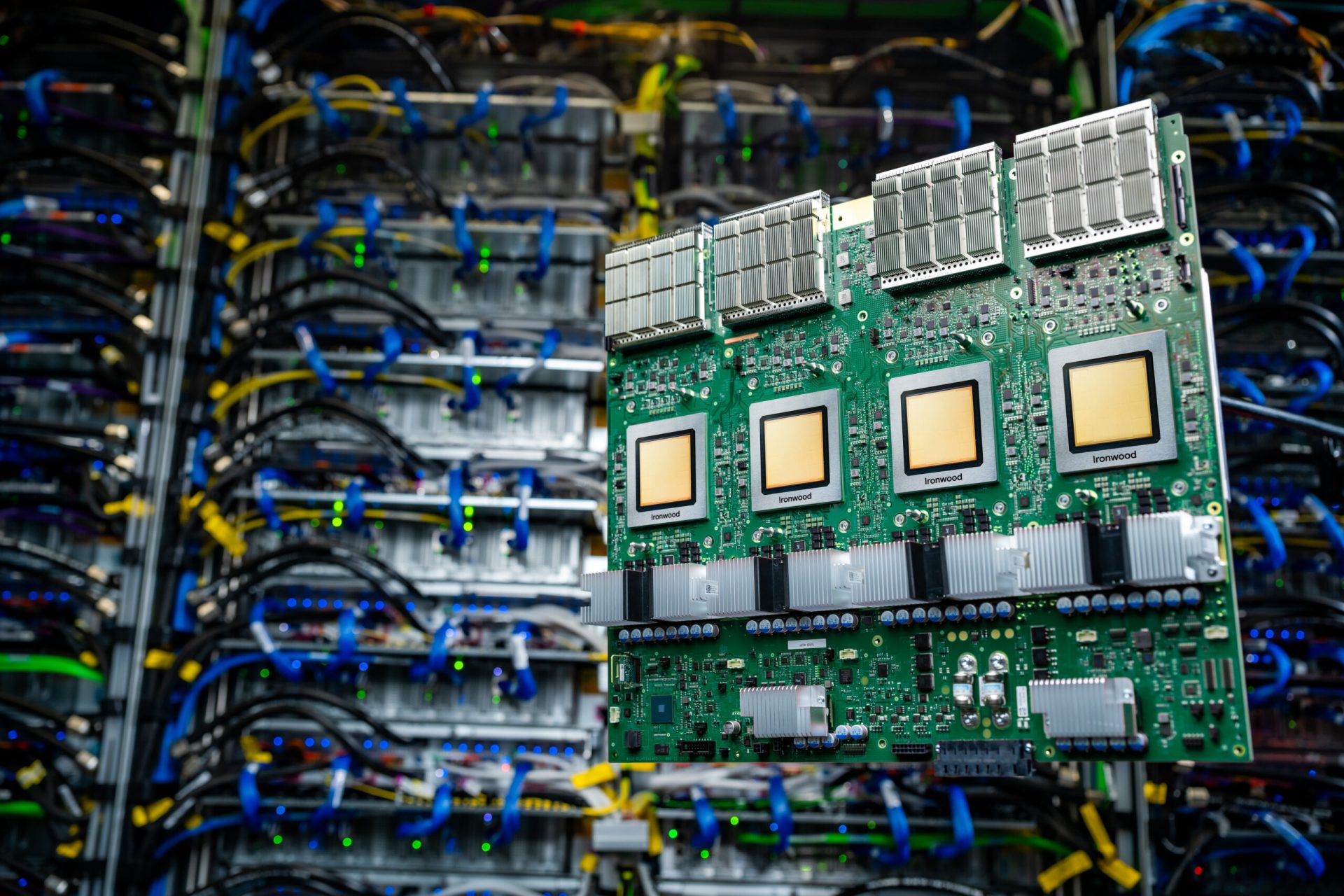
In modern chip designs, especially high-performance AI accelerators, different parts of a processor can be manufactured separately and then combined through advanced packaging. The compute tile performs heavy calculations, memory-related components help feed data to the chip, and the I/O die manages communication between the processor and the motherboard or surrounding hardware. Because each part must be carefully tuned for the manufacturer’s production equipment, the back-end design stage is critical.
This back-end design process ensures that the chip layout is compatible with the foundry’s manufacturing rules, tools, and production capabilities. For Google’s next TPU, reportedly codenamed “Icefish,” Samsung is now said to be considering outside partners to handle this back-end design work.
Several South Korean semiconductor design firms are reportedly being considered for the project, including ADTechnology, Gaonchips, and Alphachips. These companies specialize in chip design services and could help Samsung prepare the I/O die for efficient production.
The move comes as Samsung’s foundry business is said to be seeing stronger demand from companies seeking advanced chip manufacturing capacity. Reports from South Korea have suggested that Samsung is gaining attention from major AI and semiconductor customers as demand for cutting-edge manufacturing continues to rise. Some industry sources claim that orders TSMC cannot accommodate at advanced nodes may be shifting toward Samsung, especially as AI chip demand accelerates.
Google’s TPU supply chain also appears to involve other major technology partners. MediaTek has been mentioned in connection with the project, particularly around advanced chip packaging. Reports have suggested that MediaTek has been evaluating Intel’s EMIB-T packaging technology for use in the TPU, though analysts believe any adoption would depend heavily on production yield and reliability.
At the same time, there are still conflicting views across the industry about which companies will manufacture each part of Google’s next AI chip. Some financial analysts have described reports of Intel’s direct involvement in Google’s TPU manufacturing as speculative. Others have suggested that TSMC may still produce both the I/O die and compute die, using its N3 process family for the I/O component and N2-class technology for the compute portion.
If Samsung does secure the I/O die manufacturing role and outsources back-end design to a local partner, it would highlight the increasingly complex nature of AI chip production. Instead of relying on a single company to build an entire processor, major tech firms are now working with multiple foundries, design houses, and packaging specialists to create powerful custom silicon.
For Samsung, participation in Google’s TPU program would be a meaningful opportunity in the fast-growing AI semiconductor market. As demand for AI accelerators continues to expand across cloud computing, generative AI, and enterprise data centers, winning even a portion of a high-profile chip project could strengthen Samsung’s position against TSMC in advanced foundry services.
Google’s next-generation TPU is expected to be closely watched by the semiconductor industry, not only because of its role in AI computing but also because of the companies involved in its production. The project could offer a clearer look at how future AI chips will be built: through a mix of advanced nodes, specialized chiplets, custom I/O designs, and cutting-edge packaging technologies.