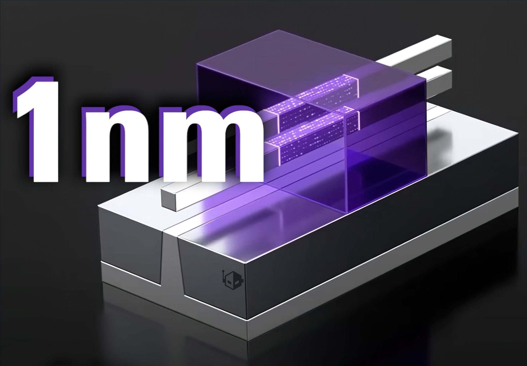
Samsung Foundry to Unveil Advanced 1nm Process Node, Eyeing Mass Production by 2026
In the highly competitive semiconductor industry, Korean tech giant Samsung Foundry is gearing up to unveil its latest technological feat—a 1nm process node. Anticipated to be presented next month, this advancement is expected to catapult Samsung to the forefront of the semiconductor manufacturing race, setting the stage for mass production in 2026.
Samsung Foundry Targets Mass Production of Next-Generation 1nm Process by 2026
The race to develop the next generation of semiconductor technologies has heated up with Samsung’s announcement to reveal their state-of-the-art 1nm process node. This move will place Samsung Foundry among the key industry players pushing the boundaries of chip manufacturing capabilities.
The forthcoming Foundry Forum & SAFE Forum 2024, scheduled to occur in the US from June 12-13, will mark a pivotal moment for Samsung as they lay out the roadmap for their 1nm process node. The Korean media’s announcements have sparked lively discussions regarding Samsung Foundry’s advancement in the market, positioning them as a formidable competitor against giants like Intel and TSMC.
Samsung’s adjusted timeline now indicates a faster transition to advanced manufacturing, with the aim to introduce the 1nm node ahead of Intel Foundry’s planned 10A (equivalent to 1nm) process in 2028 and TSMC’s expected 1nm technology by 2030. By accelerating its schedules, Samsung could potentially outpace its rivals by several years, provided they meet their promised quality and performance standards.
What Does Samsung’s 1nm Node Mean for Computing and Semiconductors?
Although details about Samsung’s 1nm node remain limited, such progress is typically associated with remarkable leaps in computing power and energy efficiency. The semiconductor industry closely watches the development of these ultra-fine process nodes, as each step forward offers potential for more powerful and efficient devices.
The broader implications of Samsung’s 1nm technology will likely extend beyond sheer computational speed, aligning with current industry trends that emphasize architectural innovation as a key driver of performance improvements. In the age of AI and advanced computing, minimizing silicon real estate through process shrinkage is important, but it is increasingly being complemented by significant architectural optimizations.
Embracing Moore’s Law and the Future of Semiconductor Design
Samsung’s developments affirm that Moore’s Law, which predicts the doubling of transistors on a chip approximately every two years, continues to be a guiding principle in the industry, despite questions about its relevance in modern semiconductor design. The continuous push for miniaturization of components goes hand in hand with refining other aspects of chip architecture, enhancing overall computing efficiency and accommodating the growing demands of AI-driven computing and other sectors.
In summary, Samsung Foundry is setting a brisk pace for the future of chip manufacturing with the introduction of its 1nm process node. The implications of this technological progress are likely to be far-reaching, driving innovations across various realms of digital technology. As Samsung unveils its roadmap for this ground-breaking technology, the industry eagerly anticipates the new milestones that the company is poised to achieve in semiconductor manufacturing.