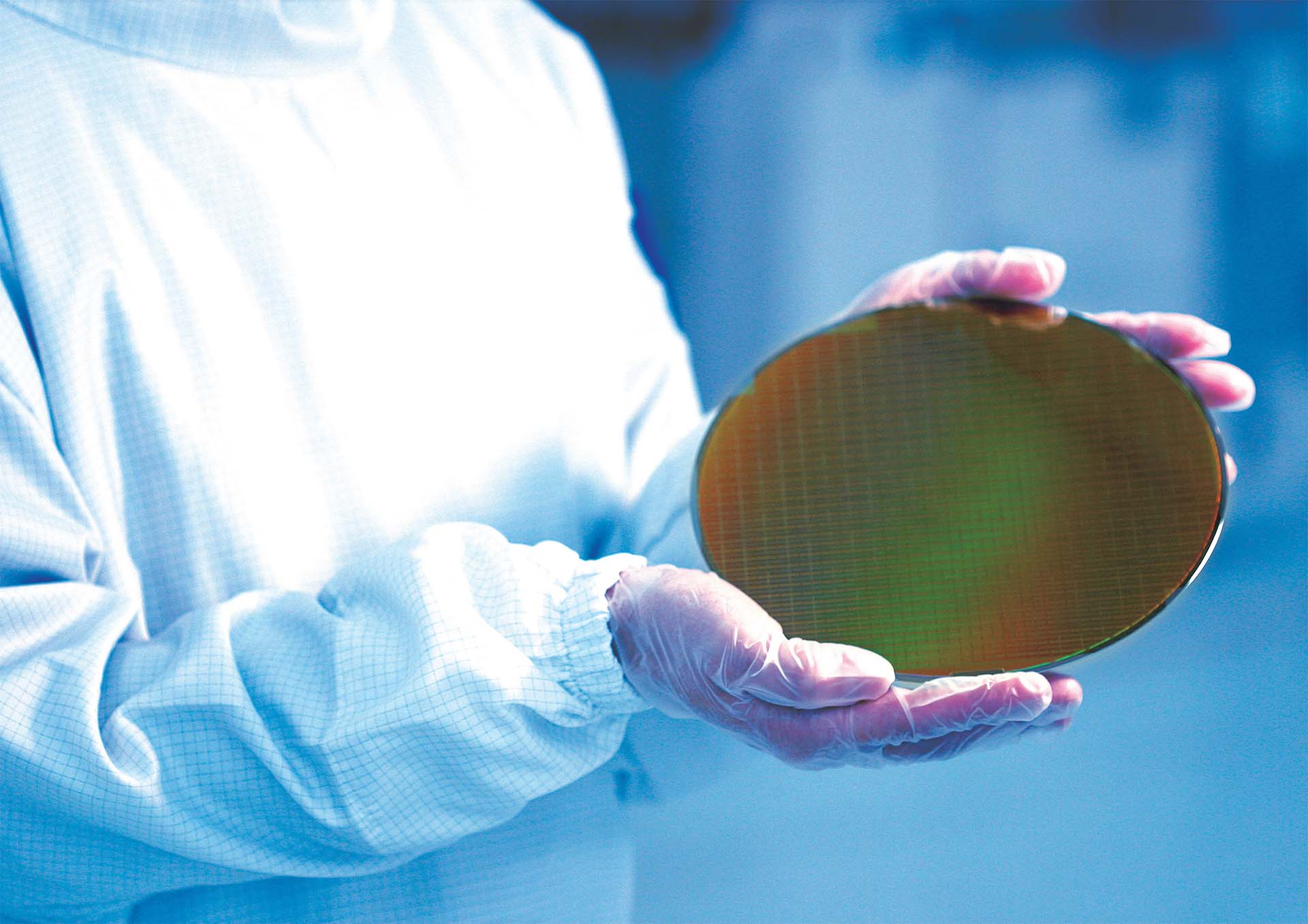
Samsung is making notable strides with its first-generation 2nm GAA (Gate-All-Around) process, signaling a rejuvenation in the foundry sector and positioning itself to challenge industry leader TSMC in the coming years. Excitingly, the Korean tech giant has reportedly completed the basic design for its next-generation 2nm GAA technology, which promises to enhance various applications, including future Exynos SoCs.
The first-generation 2nm GAA yields are gradually improving. If the development stays on track, Samsung could leverage this advanced node for its anticipated Exynos 2700. Known as SF2P, a report from ZDNet notes Samsung’s ambition to revitalize its foundry competitiveness using this advanced process. With mass production of an Exynos 2600 prototype in play, Samsung’s LSI and semiconductor teams aim for a 50% yield in the near future. Promotional efforts for SF2P technology are already in motion, suggesting a strong forward trajectory.
The goal is to begin mass production by next year. If successful, Samsung’s second-generation 2nm GAA node could become integral to future Exynos chipsets. Compared to the initial version, SF2P offers several enhancements: a 12% boost in performance, a 25% reduction in power consumption, and an 8% decrease in area. While the report doesn’t detail potential customers, there is speculation that Qualcomm might be interested.
Qualcomm is reportedly planning to use Samsung’s advanced 2nm GAA wafers for its Snapdragon 8 Elite Gen 2, destined for the Galaxy S25 series. This move suggests a potential revival of Qualcomm’s dual-sourcing strategy between Samsung and TSMC. Meanwhile, the focus remains on the first-generation 2nm GAA node, as competition in this arena could drive significant advancements and innovation among leading foundry players.