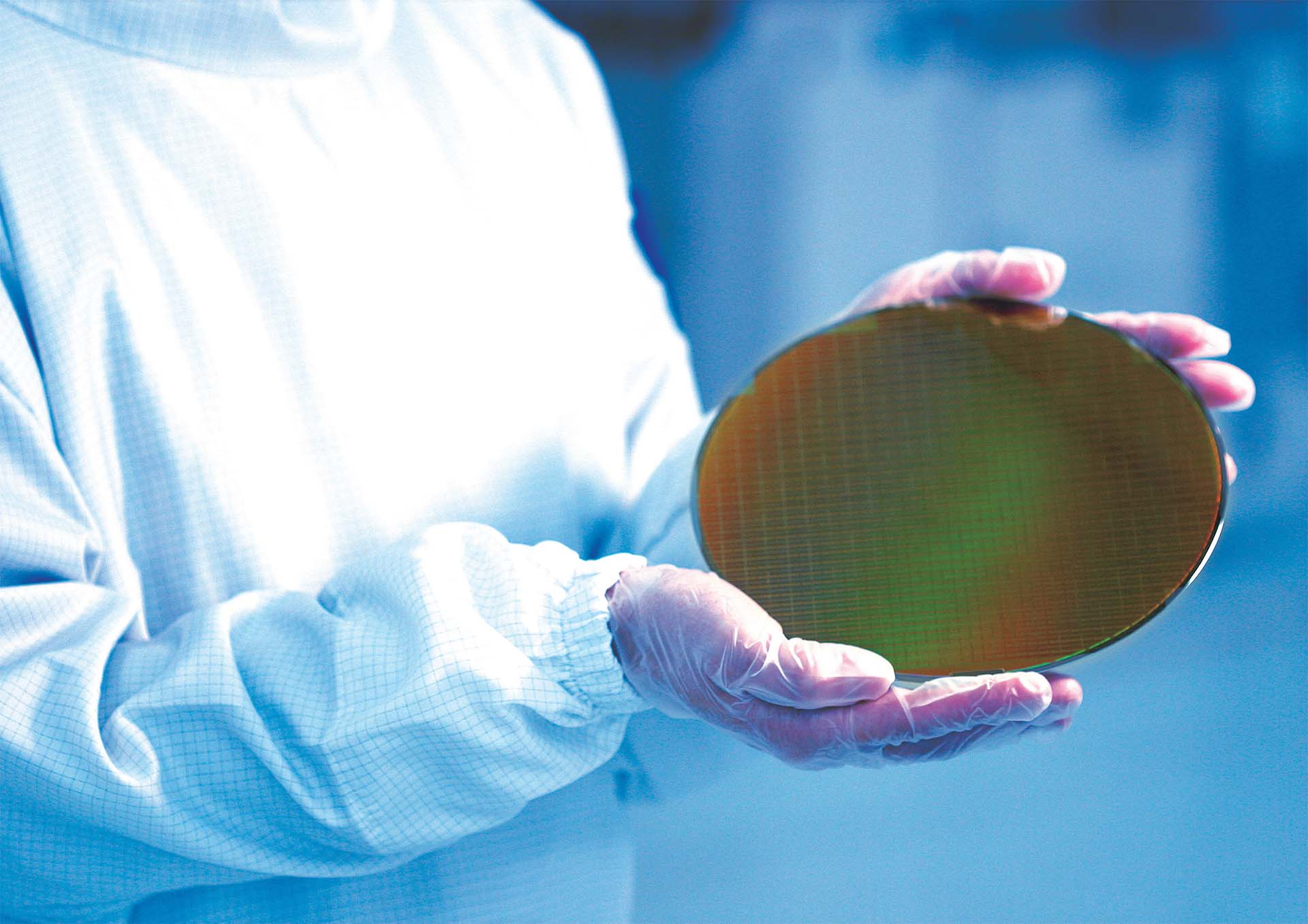
Samsung’s next big chip milestone is starting to look a lot more realistic. A new report claims Samsung Foundry has reached around a 50 percent yield on its 2nm GAA (Gate-All-Around) process—an important sign that the company’s most advanced manufacturing roadmap is moving in the right direction. Alongside that progress, Samsung is reportedly urging partners and customers to focus attention on SF2P, its second-generation 2nm GAA node, which is positioned as a more refined and improved version of the original SF2 process.
Yield is one of the biggest make-or-break factors in semiconductor manufacturing. Even if a node is technically impressive, low yields can make chips too expensive or too difficult to produce at scale. Earlier expectations suggested Samsung’s first-generation 2nm GAA would be targeting a 70 percent yield, but the latest information indicates the company is still sitting at roughly 50 percent. While that might sound modest, it still represents a notable leap over Samsung’s 3nm GAA efforts, which reportedly struggled to get beyond the 30 percent range—an issue that made it harder for the foundry to win and keep major customers.
What’s especially interesting is where Samsung appears to be placing its bets next. Rather than focusing solely on squeezing more yield out of the first-generation SF2 node, the company is said to be shifting more attention toward SF2P. Sources familiar with Samsung’s plans indicate the foundation is already in place: the basic process design kit (PDK), a crucial toolset used by chip designers to build and validate products for a manufacturing node, was reportedly completed around mid-last year. That’s a key step, because it enables ecosystem partners to start serious design work—and it signals Samsung’s intent to move faster with the newer iteration.
Samsung is also said to have issued guidance to its Design Solution Partners (DSPs) to actively promote SF2P over SF2. If accurate, that’s a strong hint that Samsung plans to allocate more resources toward SF2P ramp-up, positioning it as the more appealing option for current and future clients looking at 2nm manufacturing.
On the product side, SF2P could play a central role in upcoming next-generation chips. The report suggests Samsung’s next flagship mobile processor, the Exynos 2700, may be built on SF2P and could introduce support for newer memory and storage standards such as LPDDR6 RAM and UFS 5.0. For smartphone users, that kind of upgrade typically points to gains in bandwidth, efficiency, and overall device responsiveness—especially for AI-heavy workloads, high-resolution video, and gaming.
Beyond smartphones, there are claims that Tesla’s next AI-focused chip, referred to as AI6, may also be mass-produced using Samsung’s SF2P node. This follows talk of a major multi-billion-dollar agreement between the two companies, potentially giving Samsung a high-profile customer in an increasingly competitive AI silicon market.
Another signal of momentum: two Chinese cryptocurrency mining equipment makers, MicroBT and Canaan, are reportedly placing 2nm GAA chip orders with Samsung. Whether those projects are large-volume or more exploratory, the interest itself suggests Samsung’s 2nm roadmap is attracting attention across multiple industries—mobile, AI, and specialized compute.
Even with these encouraging signs, Samsung still has a lot of work ahead. Closing the gap with the world’s leading foundry players takes years of consistent yield improvements, strong customer execution, and reliable high-volume manufacturing. Still, Samsung appears focused on building a stronger foundation, with an internal goal of reaching profitability by 2027. If SF2P delivers the improvements it’s promising, it could become an important step in Samsung’s push to re-establish itself as a top-tier choice for cutting-edge 2nm chip production.


