Samsung Prepares Major Hybrid Bonding Line for Next-Generation HBM and Logic Chips
Samsung Electronics is reportedly moving forward with plans to build a die-to-wafer hybrid bonding production line at its Pyeongtaek campus, a key step in the company’s push to strengthen its position in advanced semiconductor manufacturing.
The new line is expected to include around 50 bonders, equipment used in the hybrid bonding process to connect semiconductor dies directly to wafers. This technology is becoming increasingly important as chipmakers race to produce faster, more efficient, and more compact processors for artificial intelligence, high-performance computing, and next-generation memory products.
Hybrid bonding is seen as a critical technology for future high-bandwidth memory, commonly known as HBM, as well as advanced logic chips. Unlike conventional packaging methods, die-to-wafer hybrid bonding allows chips to be stacked and connected with much finer precision. This can improve data transfer speeds, reduce power consumption, and support more complex chip designs.
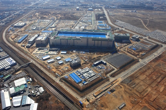
Samsung’s Pyeongtaek campus is already one of the company’s most important semiconductor hubs, housing large-scale production facilities for memory and logic chips. Adding a dedicated hybrid bonding line there would give Samsung more control over advanced packaging development and help it prepare for rising demand from AI accelerators, data centers, and premium computing platforms.
The timing is significant. Demand for HBM has surged as artificial intelligence systems require massive memory bandwidth to process large models and complex workloads. Major semiconductor companies are investing heavily in advanced packaging because performance gains are no longer driven by traditional chip scaling alone. Technologies such as hybrid bonding are now becoming essential to building the next generation of powerful and efficient chips.
For Samsung, the planned investment could help close gaps with competitors in the fast-growing HBM market while also supporting its broader foundry ambitions. Advanced packaging is increasingly viewed as a key differentiator for chip manufacturers, especially as customers look for complete solutions that combine memory, logic, and packaging expertise.
If completed as planned, the Pyeongtaek hybrid bonding line could play an important role in Samsung’s future semiconductor roadmap. With around 50 bonders expected to support production, the facility may serve as a foundation for scaling advanced chip packaging technologies across memory and logic applications.
As AI, cloud computing, and high-performance devices continue to drive demand for faster semiconductors, Samsung’s focus on die-to-wafer hybrid bonding highlights how the chip industry is shifting toward more advanced integration methods. The company’s next move at Pyeongtaek could become a major part of its strategy to compete in the next era of semiconductor innovation.


