SK Hynix is preparing HBM for the 3D packaging era with Intel EMIB, hybrid bonding, and new cooling technologies
SK Hynix is pushing deeper into advanced packaging as demand for high-bandwidth memory continues to surge across AI accelerators, GPUs, and data center processors. During a Hot Chips 2026 presentation, Jaesik Lee of SK Hynix outlined how the company plans to scale future HBM products using technologies such as improved MR-MUF packaging, hybrid bonding, Intel EMIB-style 2.5D integration, and eventually full 3D stacking with logic chips.
The message was clear: HBM is no longer just about stacking more DRAM dies. As AI workloads demand more bandwidth, higher capacity, and better energy efficiency, the packaging around HBM is becoming just as important as the memory itself.
Today’s HBM is built as a 3D stack of DRAM dies connected to a base die using through-silicon vias, commonly known as TSVs. These vertical connections allow data to move through the stack at extremely high speeds while keeping the package compact. Current HBM designs can reach up to 16-Hi stacks, meaning 16 DRAM layers are stacked together.
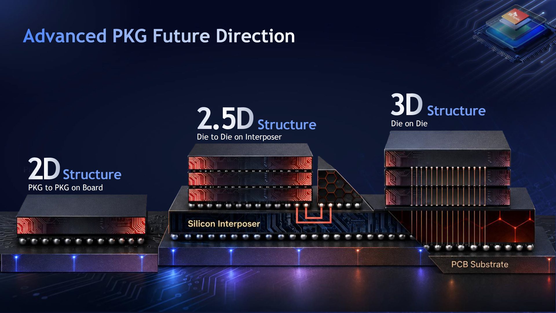
In a typical 16-Hi HBM stack, there are four ranks, with four slices per rank. Each slice includes four channels and a total of 16 banks. The HBM stack and the GPU or accelerator are separate chips, but they sit side by side on a silicon interposer using 2.5D packaging. Each HBM module can include 1,024 I/Os across 16 channels, connecting the memory to the processor through a physical interface.
This packaging approach is one of the key reasons HBM has become essential for AI and high-performance computing. Compared with traditional GDDR memory, HBM delivers far higher bandwidth in a much smaller footprint. For example, a GDDR6 configuration may offer 24 GB of memory and around 768 GB/s of bandwidth, while an HBM3E solution with four stacks can provide up to 144 GB of capacity and around 4 TB/s of bandwidth while using significantly less board space.
SK Hynix’s roadmap is now focused on HBM4, which is expected to become the company’s next flagship memory solution. HBM4 is designed to offer up to 24 Gb DRAM densities, capacities reaching 36 GB per stack, 2,048 I/O bits, I/O speeds of up to 8 Gbps, and bandwidth of around 2,048 GB/s per stack.
Compared with HBM3E, HBM4 introduces a larger package, more TSVs, more micro-bumps, and higher stack complexity. SK Hynix highlighted several key targets for HBM4, including more than 2 TB/s of bandwidth, over 40% improvement in power efficiency, more than 14% improvement in thermal resistance compared with HBM3E, and capacities of up to 48 GB. The company is preparing 12-Hi HBM4 for production, while 16-Hi versions are still going through qualification.
The package dimensions are also becoming more demanding. SK Hynix listed a 775-micron Z-height, a 12.8 x 11 mm package footprint, 16,148 base micro-bumps, and more than 20,000 TSVs. These numbers show just how dense future HBM packages are becoming.
To build these stacks, the industry currently relies on two major HBM packaging methods: thermo-compression bonding with non-conductive film, known as TC+NCF, and mass reflow with molded underfill, known as MR-MUF.
TC+NCF offers better resistance against die warpage, which is a major concern when stacking very thin memory dies. However, it has higher thermal resistance and lower productivity. MR-MUF, on the other hand, provides better manufacturing productivity and lower thermal resistance, but it is more vulnerable to chip warpage and can face challenges with gap filling between dies.
SK Hynix has already adopted advanced MR-MUF technology for its 16-Hi HBM3E solution. The company is using new techniques for warpage control, finer pitch interconnection, and narrow gap filling. With these improvements, SK Hynix has increased total package height to 775 microns while reducing chip thickness, gap height, and bump pitch.
However, scaling HBM beyond today’s limits brings serious challenges. The first major issue is power. As bandwidth increases, power consumption rises, putting more strain on the power delivery network. The second major issue is heat. More bandwidth and more layers mean higher power density, and that heat must be removed efficiently to maintain performance and reliability.
TSV area is another growing concern. Even though TSV pitch continues to shrink, the total number of TSVs is rising quickly. That means TSVs still take up a larger area inside the package. SK Hynix noted that bandwidth tends to nearly double every two generations, but this creates roughly 2.2 times more thermal burden on existing packaging technologies.
To solve these problems, SK Hynix is looking beyond conventional packaging and moving toward hybrid bonding. Hybrid bonding can enable much finer connection pitches, improved thermal conductivity, and better scaling beyond 16-Hi HBM stacks. According to SK Hynix, hybrid bonding can allow a 24% thicker core die and a TSV pitch below 18 microns compared with MR-MUF processes. Even with more stacked layers, hybrid bonding can reduce thermal resistance by around 35%.
Cooling is another area where SK Hynix is investing heavily. The company is developing a localized hotspot mitigation approach called I-HBM. This technology places a high-thermal-conductivity, electrically insulating cooling component near the HBM die-to-die PHY area, where hotspots are likely to form. By creating a dedicated heat path, I-HBM can provide more than 30% additional reduction in thermal resistance.
This is especially important as HBM moves closer to logic chips and accelerators. When memory and compute are packed more tightly together, heat becomes harder to manage. Future AI accelerators will need not only faster memory, but also packaging that can remove heat without limiting performance.
SK Hynix is also planning to boost bandwidth by increasing the number of TSVs and raising I/O speeds through logic process integration. Power delivery challenges may be addressed by using optimized logic foundry processes and spreading power TSVs throughout the package to strengthen the power delivery network.
The company also discussed how different 2.5D advanced packaging platforms affect HBM and interposer stress in different ways. SK Hynix referenced packaging approaches such as Intel EMIB and several interposer-based solutions as part of the broader industry movement toward more advanced HBM integration.
The long-term goal is full 3D integration, where HBM could eventually be stacked directly on top of accelerators. This would be a major shift from today’s 2.5D approach, where HBM sits beside the compute chip on an interposer. Stacking memory directly over logic could dramatically improve bandwidth and reduce latency, but it will require major progress in thermal design, materials, bonding, power delivery, and manufacturing reliability.
As HBM stacks move toward 16-Hi, 20-Hi, and beyond, the industry will need tighter collaboration between memory makers, chip designers, foundries, packaging specialists, and system manufacturers. Future HBM products will depend on co-optimization across design, materials, interposers, customer platforms, and cooling technologies.
SK Hynix’s roadmap shows that the race for faster AI memory is no longer only about DRAM density or raw bandwidth. Advanced packaging is now at the center of HBM innovation. Technologies such as MR-MUF, hybrid bonding, improved micro-bumps, advanced TSV layouts, localized hotspot cooling, Intel EMIB-style integration, and future 3D stacking will determine how far HBM can scale in the coming years.
For AI servers, GPUs, and next-generation accelerators, this evolution could deliver the higher capacity, higher bandwidth, and better energy efficiency needed to support increasingly demanding workloads. As the industry moves into the 3D packaging era, SK Hynix is positioning advanced HBM packaging as one of the most important foundations for future high-performance computing.