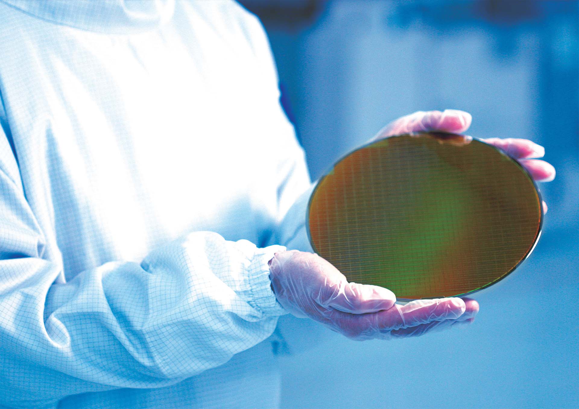
Samsung is preparing to significantly expand its advanced chip manufacturing capacity in the United States, with plans to boost 2-nanometer production at its Taylor, Texas semiconductor plant to 6,000 wafers per month.
The move is part of Samsung’s broader strategy to strengthen its foundry business and build a larger manufacturing footprint in the U.S. The company’s Taylor facility has become a key piece of that plan, especially as demand continues to rise for cutting-edge chips used in artificial intelligence, high-performance computing, mobile devices, data centers, and next-generation consumer electronics.
Samsung’s first production line at the Taylor site, often referred to as Taylor Fab 1, is expected to become operational by the end of 2026. The facility will use advanced extreme ultraviolet lithography, better known as EUV, which is essential for producing the most sophisticated semiconductor nodes.
The company has reportedly started placing additional equipment orders to support 2nm chip production at the Texas plant. These new orders are expected to help Samsung reach an initial 6,000 wafers per month for its 2-nanometer process. This comes after earlier procurement plans aimed at supporting around 10,000 wafers per month.
Once pilot production capacity is included, Samsung’s Taylor facility could eventually scale toward a maximum output of about 20,000 wafers per month by the second half of 2027.
The expansion highlights Samsung’s push to compete more aggressively in the global foundry market. The 2nm process is currently one of the most advanced semiconductor technologies in the industry, and major chipmakers are racing to bring it into high-volume production. Samsung, TSMC, and Intel are all working on 2nm-class manufacturing, with each company using its own approach to transistor design and production strategy.
Samsung’s 2nm technology relies on gate-all-around field-effect transistors, commonly known as GAAFETs. The company refers to its version as Multi-Bridge Channel FET, or MBCFET. This design uses nanosheets as the channel material, allowing the gate to wrap more effectively around the channel and control electrical current with greater precision.
This transistor structure is designed to improve performance, reduce power consumption, and allow chips to become more efficient as traditional FinFET designs reach their physical limits. For customers building AI accelerators, mobile processors, and advanced computing chips, improvements in power efficiency and performance are becoming increasingly important.
Samsung’s investment in Taylor, Texas also reflects the growing importance of domestic semiconductor manufacturing in the United States. Governments and technology companies are increasingly focused on creating more resilient chip supply chains after years of global shortages and rising geopolitical concerns.
By expanding 2nm production capacity in Texas, Samsung is positioning itself to serve major U.S.-based chip designers that want access to advanced manufacturing closer to home. If the company can meet its production timeline and improve yields, the Taylor fab could become a major hub for leading-edge semiconductor manufacturing in North America.
The coming years will be critical for Samsung’s foundry ambitions. Scaling 2nm production is technically challenging, and success will depend on equipment readiness, process stability, customer demand, and yield improvements. Still, the latest equipment orders suggest Samsung is moving forward with a clear plan to grow its U.S. chipmaking capacity and compete more directly in the race for next-generation semiconductor production.