Lawrence Livermore National Laboratory (LLNL) is on the cutting edge of laser technology with the development of a revolutionary petawatt-class laser system. This new innovation, called the Big Aperture Thulium (BAT) laser, holds the potential to dramatically enhance the efficiency of EUV lithography equipment critical for chip manufacturing. Compared to the CO2 lasers that currently lead the industry, the BAT laser could deliver a tenfold increase in efficiency.
This groundbreaking project is part of a four-year, $12 million initiative at the Extreme Lithography & Materials Innovation Center (ELMIC), supported by the Department of Energy’s Microelectronics Science Research Centers program. It represents a collaborative effort with partners like the SLAC National Accelerator Laboratory, ASML San Diego, and the Advanced Research Center for Nanolithography.
The BAT laser differentiates itself by utilizing thulium-doped yttrium lithium fluoride as its gain medium, operating at a novel wavelength of approximately 2 microns. This contrasts with the common 1 or 10 micron wavelengths of current lasers. The unique wavelength could significantly improve the efficiency of converting plasma into EUV light by interacting with tin droplets during the lithography process.
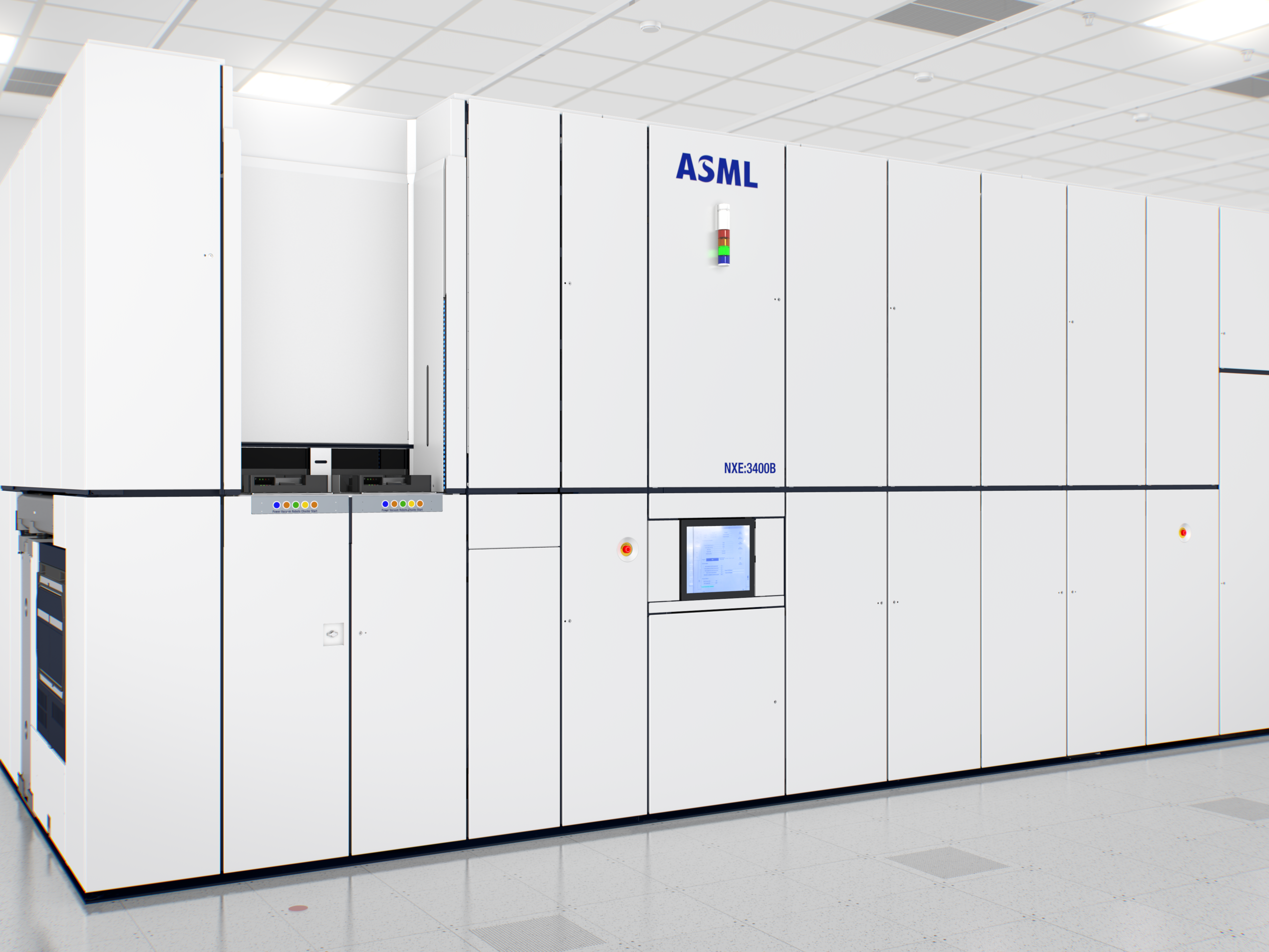
EUV lithography systems today demand immense amounts of power, up to 1,400 kilowatts for high numerical aperture (NA) EUV tools. The bulk of this energy is needed to heat tin droplets to an extraordinary 500,000°C, creating plasma that emits the crucial 13.5-nanometer light. The deployment of the BAT laser, with its diode-pumped solid-state technology, promises better energy efficiency and heat management than existing CO2 laser systems.
Leading this ambitious project are laser physicist Brendan Reagan and plasma physicist Jackson Williams, who bring with them a foundation of five years of plasma simulations and preliminary tests that have already captivated the EUV lithography industry.
Research and testing are set to take place at LLNL’s Jupiter Laser Facility, which has recently undergone an extensive four-year upgrade. This site is part of LaserNetUS, a network of high-power laser laboratories across North America, funded by the Department of Energy’s Office of Science.
The transition to BAT laser technology could accelerate chip production and decrease power consumption; however, the deployment in the semiconductor sector poses significant challenges. Adapting current infrastructure is no small feat, and such changes won’t happen overnight. It’s worth remembering that the journey to produce today’s EUV systems took decades from inception to market readiness. Nonetheless, this advancement holds exciting possibilities for the future of chip manufacturing.


