Rapidus Expands Hokkaido Semiconductor Hub With 2nm Chip Development, Packaging, and Analysis Capabilities
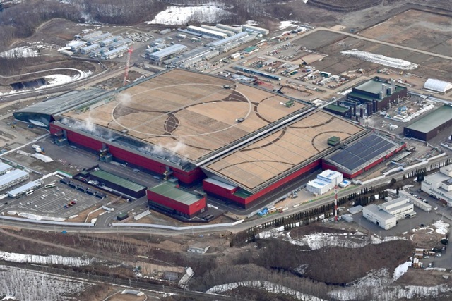
Rapidus is strengthening its semiconductor ambitions in Japan by expanding the development and production network surrounding its Chitose foundry in Hokkaido. The company is adding new chip analysis and advanced packaging capabilities to support its front-end pilot line for next-generation 2nm logic chips.
The move marks another important step in Japan’s effort to rebuild a strong domestic semiconductor supply chain. By bringing multiple stages of chip development closer together, Rapidus aims to create a more efficient ecosystem for designing, testing, manufacturing, and packaging cutting-edge processors.
At the center of this expansion is the company’s Chitose facility, which is being positioned as a key hub for advanced semiconductor manufacturing. The site is expected to play a major role in developing 2nm logic chip technology, a process node that could power future high-performance computing, artificial intelligence, automotive systems, data centers, and advanced consumer electronics.
Adding chip analysis capabilities is especially important for a project of this scale. As semiconductors become smaller and more complex, manufacturers need precise tools to inspect, evaluate, and improve each stage of production. Advanced analysis can help identify defects, improve yields, and accelerate the transition from pilot production to larger-scale manufacturing.
Advanced packaging is another critical piece of the strategy. Modern chips are no longer judged only by how small their transistors are. Packaging technology now plays a major role in performance, power efficiency, heat management, and the ability to combine multiple chip components in compact designs. By investing in packaging near the front-end production line, Rapidus can better support the development of high-performance semiconductor products from start to finish.
The expansion also highlights the growing importance of Hokkaido as a semiconductor production region. Chitose offers room for large-scale industrial development, access to infrastructure, and a location that can support a broader technology ecosystem. As Rapidus builds out its operations, the surrounding area could attract suppliers, engineering talent, research partners, and related businesses.
For Japan, the project carries strategic significance. Semiconductors are essential to nearly every modern industry, from smartphones and electric vehicles to cloud computing and defense technologies. Developing domestic production capacity for advanced logic chips would reduce reliance on overseas supply chains and strengthen the country’s position in the global chip market.
The focus on 2nm logic chips also puts Rapidus in one of the most competitive areas of semiconductor manufacturing. Producing chips at this level requires extreme precision, advanced equipment, strong research partnerships, and deep technical expertise. The addition of analysis and packaging operations suggests the company is building a more complete foundation for long-term development rather than focusing only on wafer production.
While pilot lines are typically used to refine manufacturing processes before mass production, they are essential for proving new technologies and improving reliability. Rapidus’ front-end pilot line for 2nm chips will likely serve as a testing ground for process improvements, yield optimization, and future manufacturing strategies.
The broader goal is to create a tightly connected semiconductor cluster in Hokkaido, where research, production, inspection, and packaging can work together more efficiently. This kind of integrated approach is becoming increasingly important as chipmaking grows more complex and costly.
Rapidus’ expansion around its Chitose foundry signals that Japan’s advanced chip manufacturing plans are moving beyond concept and into infrastructure development. With new analysis and packaging capabilities being added alongside 2nm logic chip production efforts, the company is working to establish Hokkaido as a major center for next-generation semiconductor technology.