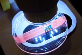
As the global semiconductor industry moves deeper into the post-Moore’s Law era, the race for better performance is no longer driven by shrinking transistors alone. With demand for artificial intelligence (AI) and high-performance computing (HPC) accelerating, advanced packaging has emerged as one of the most important battlegrounds for next-generation chips—and a major factor in national and industrial competitiveness.
A newly launched chip-level advanced packaging platform is set to strengthen Taiwan’s position in this rapidly evolving landscape. The initiative focuses on the kinds of packaging technologies now essential for modern processors, especially those used in AI training, AI inference, data centers, and other compute-heavy workloads. Instead of relying only on silicon scaling, advanced packaging enables manufacturers to combine multiple chiplets, improve interconnect speed, increase bandwidth, and manage heat more effectively—key advantages for AI-grade performance.
Why advanced packaging matters more than ever
As chips become more complex and workloads become more demanding, performance gains increasingly come from how components are assembled and connected. Advanced packaging helps deliver:
1) Higher performance through shorter, faster connections between chip components
2) Better power efficiency by optimizing data movement
3) Greater design flexibility using chiplets rather than one monolithic die
4) Improved thermal management, which is crucial for AI and HPC systems
5) Faster product iteration and better yields by mixing and matching dies
In practical terms, this manufacturing approach supports today’s most sought-after technologies: high-bandwidth memory integration, dense interconnects, heterogeneous integration, and compact multi-die designs—all vital for competitive AI hardware.
A strategic boost for Taiwan’s semiconductor ecosystem
Taiwan already plays an outsized role in global semiconductor manufacturing, and expanding capabilities in advanced packaging adds another layer of strength. A chip-level platform can help streamline R&D, enable prototyping, and accelerate the transition from research to production-ready packaging solutions. It also supports talent development and gives domestic and international partners a stronger foundation for collaboration on next-generation packaging processes.
This is particularly significant as AI demand reshapes the industry. The fastest-growing computing segments increasingly rely on packaging innovation to keep pushing performance upward while controlling power draw and heat. By investing in an advanced packaging platform now, Taiwan positions itself to stay highly competitive as the industry shifts from traditional scaling to system-level optimization.
What this signals for the future of chips
The post-Moore’s Law transition doesn’t mean innovation is slowing—it means it’s moving. Advanced packaging is becoming a decisive differentiator for chips designed for AI, HPC, and data-centric computing. Platforms that support chip-level packaging development are likely to play a central role in how quickly new architectures reach the market, how efficiently they run, and how well supply chains respond to rising global demand.
If you’d like, paste the rest of the post content (the text after the opening paragraph), and I’ll rewrite the full article with stronger SEO phrasing, smoother flow, and more specific keyword coverage while keeping the original intent.