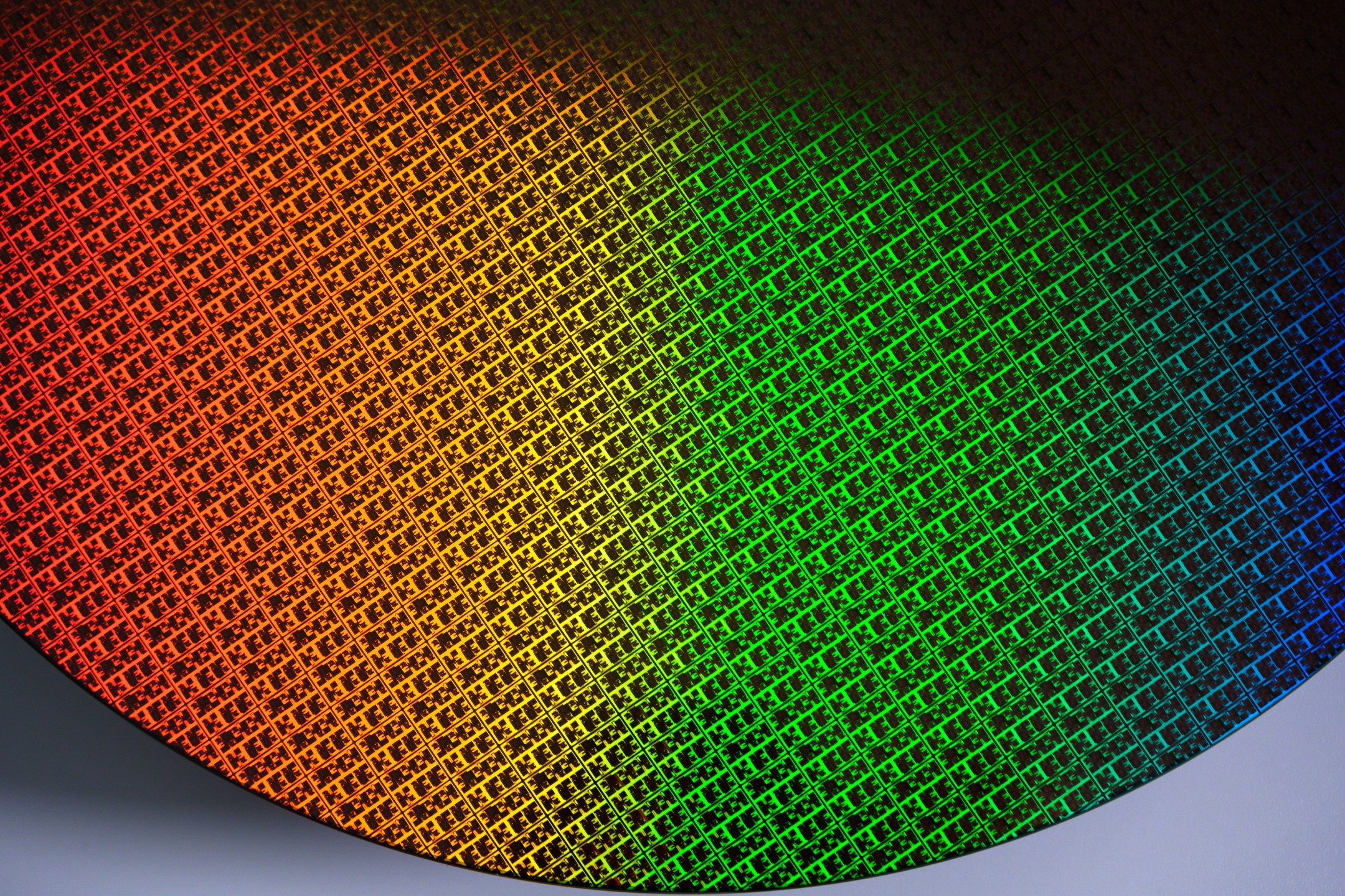
There’s a significant buzz around Intel’s innovative 18A process, heralding what could be a major leap forward for the company’s semiconductor ambitions. Reports now reveal that Intel’s 18A SRAM density matches that of TSMC’s N2 process, a testament to its impressive progress in semiconductor technology.
Intel’s 18A process is the result of dedicated research and development, showcasing particular advancements such as the Backside Power Delivery Network (BSPDN). This innovative approach relocates power delivery to the back of the wafer, enhancing power efficiency and signal integrity, marking a significant industrial milestone.
Further highlighting its achievements, Intel reports a macro bit density of 38.1 Mb/mm² for its high-density 18A versions, utilizing a larger array configuration. This data indicates promising developments, although the true test will be how well these innovations translate to large-scale chip production and whether yield rates meet expectations.
Meanwhile, TSMC is not resting on its laurels. The company has announced a 12% improvement in SRAM density with its N2 process, thanks to the integration of GAA technology, and an 18% improvement for high-performance SRAM. This shift from the traditional FinFET technology to a more customizable “nanosheet” configuration is part of what gives TSMC an edge.
The race between Intel and TSMC in the semiconductor sector is heating up, as both companies push the boundaries of technological innovation. While the competition is intensifying, the ultimate outcome will depend on how these processes perform as they are rolled out into the broader supply chain. Each step forward brings us closer to more efficient and potent computing capabilities in the AI era.