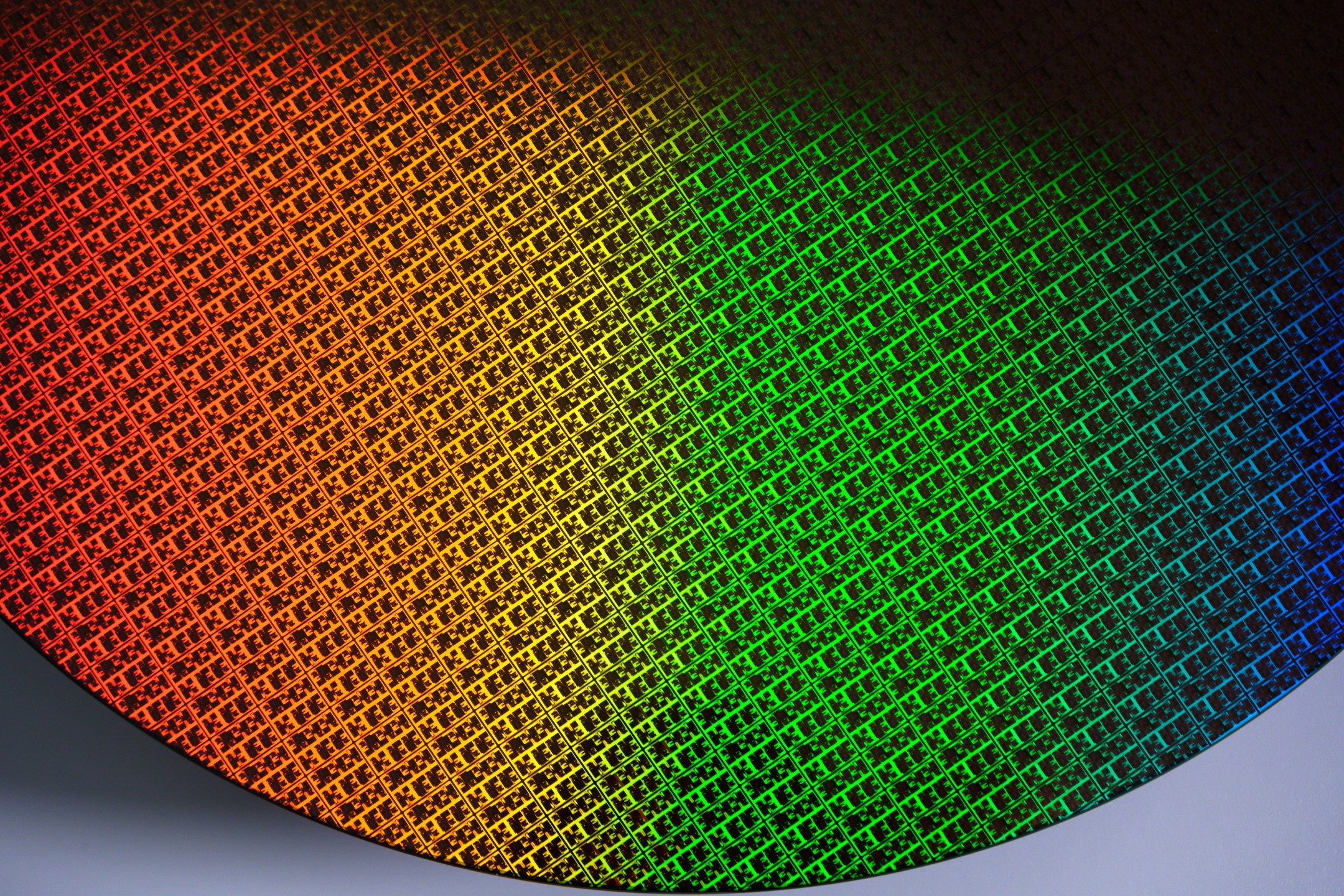
Intel’s 18A process is generating significant buzz across the tech industry as the company positions itself to reclaim leadership in the semiconductor space. Under the dynamic leadership of Pat Gelsinger, Intel has revitalized its focus on advancing its foundry technologies, and their efforts are paying off. The 18A process, which made a splash at the VLSI Symposium 2025, promises major enhancements over previous nodes, showcasing Intel’s innovative prowess.
One of the standout features of the 18A process is its ability to achieve more than a 30% improvement in density scaling when compared to the Intel 3 process. This leap is largely thanks to the integration of cutting-edge technologies such as PowerVia and BSPDN. The performance gains are equally impressive, with the 18A offering a 25% increase in speed and a 36% reduction in power consumption at a standard operational voltage of 1.1V on an Arm core sub-block.
Remarkably, the 18A process also enhances area utilization, paving the way for higher density designs. This is crucial for future advancements as it allows for more efficient use of space, ultimately enabling more powerful and compact chip designs. The introduction of a “voltage droop” map illustrates the robustness of 18A under high-performance scenarios. Thanks to the innovative PowerVia technology, 18A demonstrates a stable and efficient power delivery system, a critical factor for reliable computing power.
Additionally, Intel has made strides in area efficiency by employing backside power delivery. This shift has allowed for denser cell packing, freeing up valuable space for frontside routing. These advancements suggest that the 18A node stands out as Intel’s most capable yet, shaping up to be a formidable competitor in the industry.
A comparison with industry peers reveals that Intel’s progress with the 18A process aligns it closely with TSMC’s N2 process in SRAM density, underscoring the competitive edge that Intel is vying for. This indicates a potential shift in the balance of power in terms of semiconductor node technology.
Looking forward, the 18A process is set to power future technologies, starting with the Panther Lake SoCs and the Xeon “Clearwater Forest” CPUs. If production yield rates continue to improve, we may witness these innovations integrated into widespread products as early as 2026, marking a pivotal moment in Intel’s journey to technological eminence.


