Intel 18A-P Process Technology Moves Into Risk Production as Intel Foundry Targets AI, HPC, and Next-Gen Xeon Chips
Intel is putting more attention on its 18A-P process technology, a refined version of its 18A node that could play a major role in the company’s foundry ambitions. While Intel’s upcoming 14A process has attracted plenty of interest, 18A-P may be just as important in the near term because it is designed to give customers a practical, performance-focused path forward while building on the foundation of Intel 18A.
Semiconductor manufacturing is one of the most difficult and competitive industries in the world. Intel has been working aggressively to restore confidence in its manufacturing roadmap, especially as it expands Intel Foundry into a serious alternative for companies building advanced chips for artificial intelligence, high-performance computing, data centers, and custom silicon.
The company has already made significant progress with Intel 18A, but 18A-P is intended to push that platform further. Rather than rushing directly to the next major node, Intel is offering a more optimized process that keeps compatibility with 18A while adding meaningful performance, power, and thermal improvements.
At VLSI 2026, Intel shared a deeper look at 18A-P and confirmed that the process is now in risk production. That milestone means the technology is moving beyond early development and toward broader readiness for customers and internal products.
One of the biggest advantages of Intel 18A-P is its performance-per-watt improvement over standard 18A. According to Intel, 18A-P can deliver up to 9% higher performance at the same power, or up to 18% lower power at the same performance, based on a standard Arm core sub-block comparison. For customers developing AI accelerators, server processors, networking chips, and other advanced compute products, that kind of efficiency gain can be extremely valuable.
The process continues to use Intel’s gate-all-around transistor architecture and backside power delivery foundation. These technologies are central to Intel’s advanced manufacturing strategy. Gate-all-around transistors, branded by Intel as RibbonFET, are designed to improve transistor control and efficiency, while backside power delivery, known as PowerVia, helps reduce routing congestion by moving power lines to the back of the wafer.
A key strength of Intel 18A-P is that it remains fully design-rule compatible with Intel 18A. This matters because chip designers can reuse existing intellectual property and design flows instead of starting from scratch. For foundry customers, compatibility can reduce development time, lower risk, and make the transition to a newer process much smoother.
Intel is also positioning 18A-P as a strong option for low-voltage and energy-efficient computing. This is especially important as AI and HPC workloads continue to demand more performance while putting pressure on power budgets and cooling systems. Data centers are already struggling with rising energy consumption, and any process improvement that lowers power draw or improves thermal behavior can have a major impact at scale.
Thermals are another important part of the 18A-P story. Intel says the process includes material and design innovations that can improve thermal resistance by 20% to 40% when paired with enhanced electronic design automation workflows. Better thermal resistance can help chips sustain higher performance for longer periods and may simplify cooling requirements in dense computing environments.
Intel also reports a 10% to 30% improvement in through-silicon via resistance through geometric and material optimizations. These vertical connections are increasingly important in modern chip designs, especially as the industry moves toward advanced packaging, chiplets, and 3D integration. Lower resistance can help improve signal and power delivery efficiency inside complex semiconductor designs.
Another important addition to 18A-P is a feature Intel calls Power Boost. The company describes it as an industry-first implementation of a dual-contact architecture enabled by PowerVia backside power delivery for both NMOS and PMOS transistors. In simple terms, Power Boost is designed to increase drive current and improve frequency while keeping capacitance matched. That can help deliver better performance without requiring a larger chip footprint.
This makes 18A-P particularly attractive for power-constrained applications where designers need more frequency or efficiency within a fixed area. Intel says the process will offer both 160 nm and 180 nm cell heights, along with a 50 nm contacted poly pitch, similar to Intel 18A. It also introduces new low-power and high-performance transistor options, giving chip designers more flexibility when balancing speed, energy use, and silicon area.
Intel is also adding a fifth logic threshold voltage pair between ultra-low-voltage threshold and low-voltage threshold options. This gives designers another tuning point to optimize their chips depending on workload requirements. For advanced processors, these kinds of options can help squeeze out additional efficiency or performance in critical parts of the design.
Backside power delivery remains one of the most important differentiators for Intel’s advanced nodes. By moving major power routing to the back of the wafer, Intel can reduce congestion on the front side of the chip, where signal routing takes place. This can lead to shorter wires, fewer vias, and better overall layout efficiency. Intel says backside power can provide an 11% area reduction, while the 32 nm metal process used with 18A-P helps keep manufacturing more cost-effective and reduces some process complexity.
Beyond 18A-P, Intel also discussed several research breakthroughs that could influence future manufacturing technologies.
One area involves efficient power management logic using 300 mm gallium nitride and silicon technology. Intel researchers, working with academic collaborators, demonstrated efficient multi-thousand-gate digital control circuits built directly on a chip using a hybrid gallium nitride nMOS and silicon pMOS approach. The team achieved a record power-delay product of 6.2 attojoules per stage, which Intel says is more than 1,000 times more efficient than previous gallium nitride logic approaches. This type of technology could eventually help integrate control circuitry directly on-chip, reducing cost, size, and complexity while improving system performance.
Intel also showcased progress in CFET transistor integration at a 45 nm gate pitch using a 2×2 ribbon stack. CFET technology stacks NMOS and PMOS transistors vertically, allowing more performance and density in a smaller area. The research included working logic circuits, backside power delivery, direct backside contacts, and compact vertical connection methods. These developments point toward future transistor designs that could extend scaling beyond today’s gate-all-around architectures.
Another research area focused on next-generation interconnects using subtractive ruthenium wiring with airgaps. Intel demonstrated this metallization approach with functional RibbonFET devices on a test chip. The company says the design can deliver about a 2% circuit performance improvement at matched leakage compared with conventional copper interconnects, helped by capacitance reductions of up to 35% from the airgap. Intel also reported up to 50% lower via resistance, which could improve vertical signal connections in future chip designs.
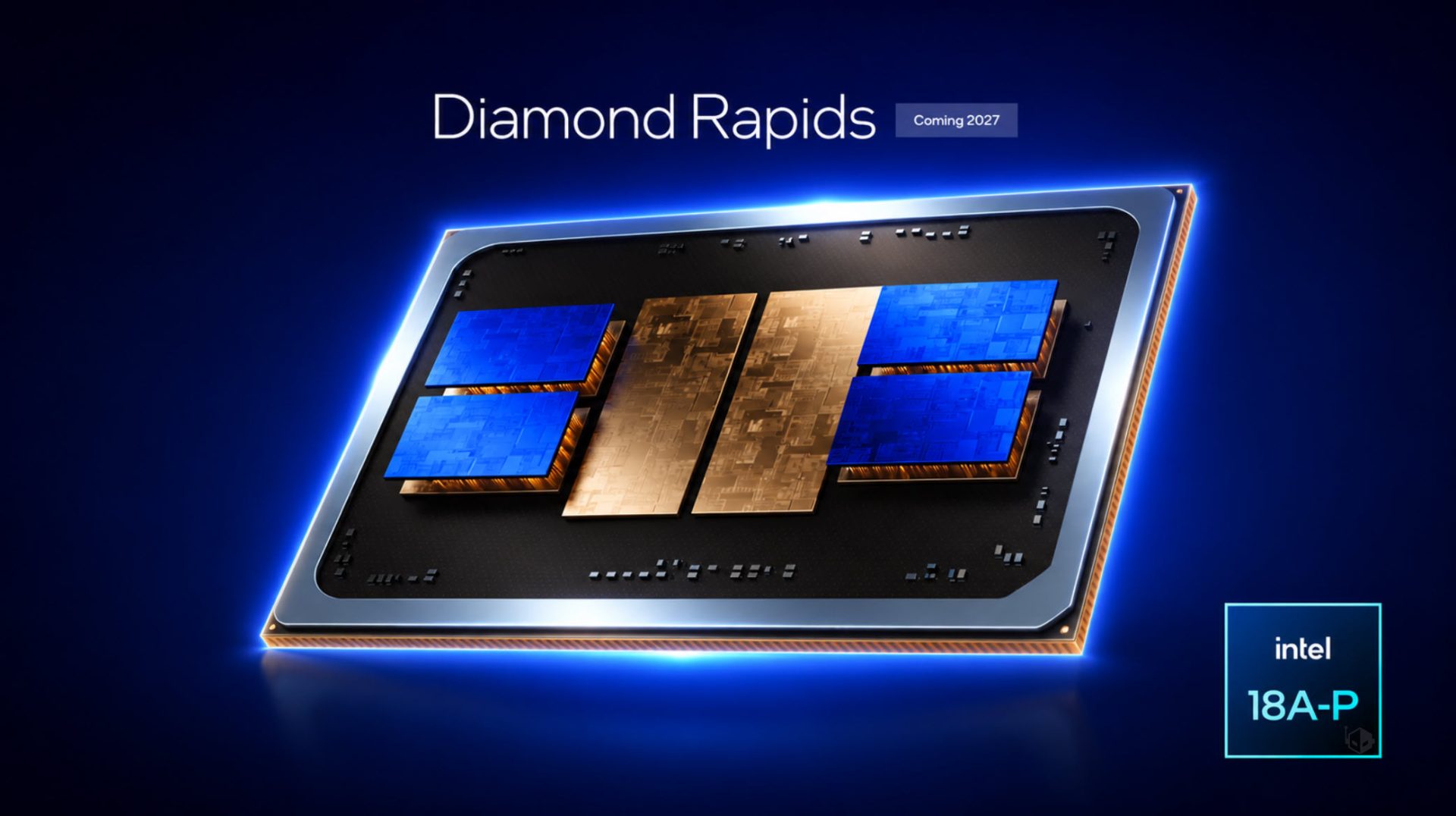
Intel’s confidence in 18A-P is also reflected in its own product roadmap. At Computex 2026, the company announced Diamond Rapids, its next-generation Xeon processor family, which will be built using Intel 18A-P. This is an important signal because Intel is not only offering the process to external customers but also using it for one of its most important data center CPU platforms.
For Intel Foundry, this is a crucial moment. The demand for advanced chips is rising quickly, driven by artificial intelligence, cloud infrastructure, custom accelerators, and high-performance computing. At the same time, supply constraints in leading-edge manufacturing remain a concern for many technology companies. If Intel can prove that 18A-P delivers reliable performance, strong yields, and competitive efficiency, it could attract more customers looking for additional manufacturing capacity.
Reports have already suggested that several major companies are evaluating or working with Intel Foundry in different ways. As the AI chip market continues to expand, the need for advanced foundry services is only expected to grow.
Intel still has plenty to prove, but 18A-P appears to be a key part of its strategy. By combining design compatibility with 18A, improved power efficiency, stronger thermal characteristics, Power Boost technology, and backside power delivery, Intel is trying to make 18A-P a practical and attractive node for next-generation chips.
If the process delivers as promised, Intel 18A-P could become one of the most important stepping stones in the company’s foundry comeback and a major technology platform for future AI, HPC, and data center silicon.