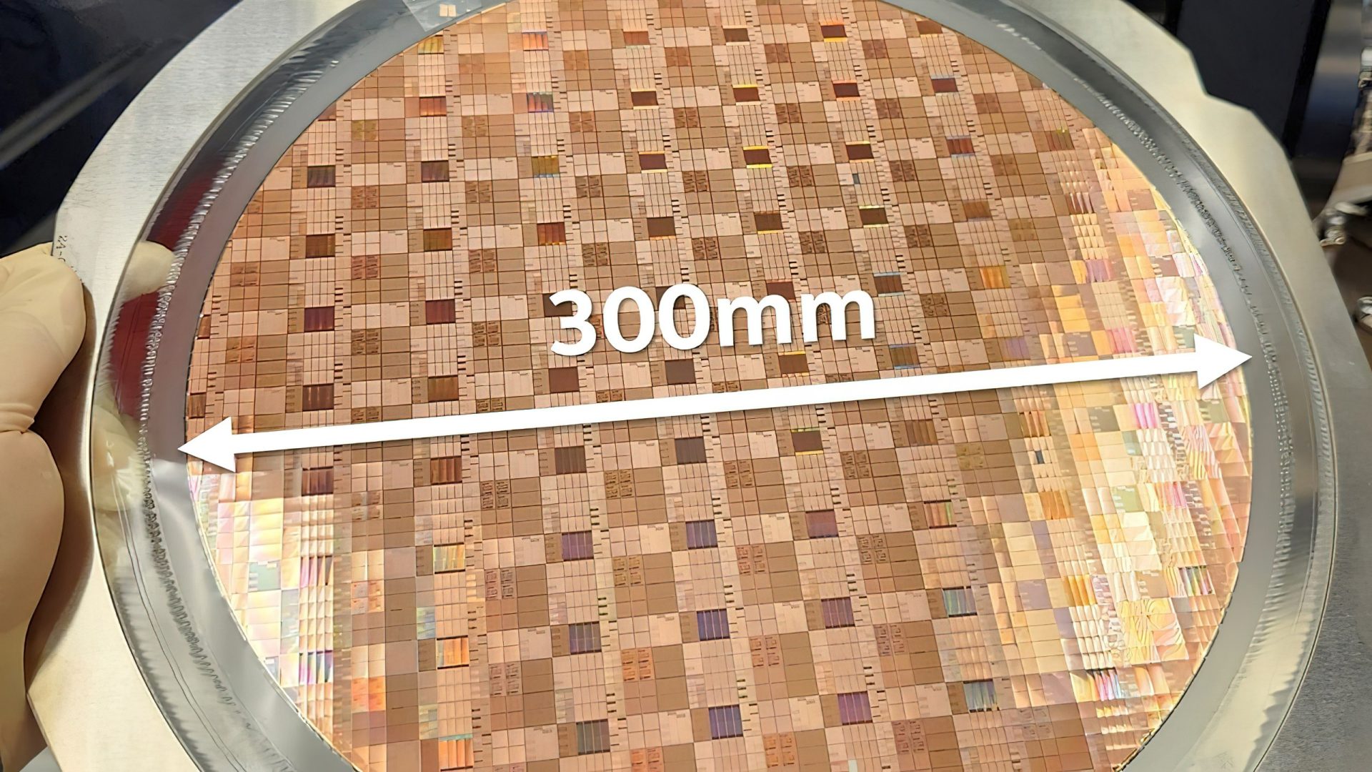
Intel Foundry has hit a major semiconductor milestone by producing what it calls the world’s first and thinnest gallium nitride (GaN) chiplet. Built from a 300mm GaN-on-silicon wafer, the chiplet’s base silicon is only 19 micrometers thick—about one-fifth the width of a human hair. The result is a tiny power-focused building block designed to deliver more speed and efficiency in the cramped, high-demand environments powering modern computing and connectivity.
This breakthrough was presented at the 2025 IEEE International Electron Devices Meeting (IEDM) and targets a problem the entire industry is wrestling with: performance keeps climbing, but space and power budgets are not. Graphics processors, servers, and network hardware all want higher power delivery and faster switching in smaller footprints. Traditional silicon approaches are increasingly constrained by physical and thermal limits, which is why GaN has become one of the most important materials in next-generation power electronics and high-frequency systems.
What makes Intel Foundry’s approach stand out is that the GaN transistors aren’t being treated as a standalone power component that needs extra chips around it to function. Researchers demonstrated GaN transistors combined with silicon-based digital circuitry on the same chip, enabling fully monolithic on-die digital control circuits built using a single integrated manufacturing flow. In practical terms, that means complex control functions can be integrated directly into the power chiplet instead of relying on a separate companion chiplet.
That integration matters because it can cut energy waste and latency that occur when signals have to travel between multiple components. Reducing routing overhead is a direct path to better efficiency, especially in systems where power regulation and fast switching are critical.
Intel also emphasizes that extensive reliability testing has been completed, with results suggesting the technology can meet the expectations needed for real-world deployment. That’s a big point for GaN adoption, because performance alone isn’t enough—power components must handle stress over time under heat, voltage, and heavy workloads.
Why ultra-thin GaN chiplets could reshape data centers and networking
Data centers are one of the clearest beneficiaries of GaN-based power delivery. GaN can switch faster and with lower losses than many silicon-based alternatives, which could lead to smaller, more efficient voltage regulators. Just as important, those regulators could be placed closer to the processor, reducing resistive losses caused by longer power delivery paths on a board. The end goal is higher efficiency and potentially less wasted energy turned into heat—an increasingly expensive problem at scale.
On the connectivity side, GaN’s high-frequency strengths make it a natural fit for radio frequency (RF) frontend hardware used in wireless infrastructure. Intel points to applications such as base stations for next-generation 5G and emerging 6G development. GaN is also attractive for systems operating in centimeter- and millimeter-wave bands, and it can remain efficient at extremely high frequencies, with the potential to exceed 200 GHz. Those capabilities can extend beyond cellular networks into radar, satellite communications, and photonics, where fast electrical switching can be used to modulate light signals.
GaN vs. silicon: why the industry is pushing beyond CMOS limits
Compared to conventional CMOS-based silicon designs, GaN chiplets offer several advantages in the areas that are becoming most critical: power density, switching efficiency, and the ability to handle harsher operating conditions. Higher power density helps deliver more capability in less space—an advantage for crowded server boards, wireless base stations, and other space-constrained platforms. Intel even frames electric vehicles as “a data center on wheels,” highlighting how the same drive for compact, high-efficiency power delivery shows up across industries.
Heat is another dividing line. Silicon can become unreliable at junction temperatures above roughly 150°C, which restricts how it can be used in high-thermal environments. GaN’s wider bandgap can support higher-temperature operation with greater stability, potentially reducing switching losses and making thermal management easier. Better efficiency can also translate into smaller cooling solutions, which can lower system size and cost.
Another key detail is manufacturing compatibility. By working with 300mm GaN-on-silicon wafers—the standard format used broadly across silicon manufacturing—Intel Foundry is aiming for a path that fits existing semiconductor infrastructure. That could reduce the need for massive, specialized retooling, making it easier for the industry to scale GaN production using familiar processes and equipment.
Taken together, the ultra-thin 19μm GaN chiplet and its integrated digital control circuitry point toward a future where power delivery becomes smaller, smarter, and more tightly integrated—exactly what next-generation data centers, high-performance computing, and advanced wireless networks will demand.