In the dynamic world of semiconductor manufacturing, advanced packaging technologies play a crucial role in the development and delivery of high-performance electronic devices. Among these innovative packaging solutions, Fan-Out Panel-Level Packaging (FOPLP) has emerged as a significant opportunity, particularly for Outsourced Semiconductor Assembly and Test companies (OSATs) and other industry entities looking to make a mark alongside giants like TSMC, Samsung Electronics, and Intel.
## The Growth of FOPLP in Semiconductor Packaging
Fan-Out Panel-Level Packaging technology is relatively new yet rapidly evolving. It stands out as a method capable of providing higher I/O density in semiconductors without increasing the package size, which is essential for meeting the needs of today’s miniaturized yet powerful electronic devices. The technology fans out the electrical contacts of a chip to a broader area on the panel for easier connection, enabling slimmer profiles and more function-packed gadgets.
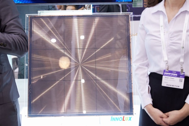
## Innolux and OSATs Innovating Together
Key players like Innolux and numerous OSATs are diving deep into the FOPLP deployment, striving to carve out their niche by leveraging this advanced packaging technology. Such a move is strategic; it not only allows them to distinguish themselves from the competition but also to offer an alternative in a sector where the big three – TSMC, Samsung, and Intel – have traditionally dominated.
## Challenges and Opportunities for FOPLP
Adopting FOPLP does present challenges, from the initial investment in new equipment to mastering the delicate processes involved. However, the prospect of gaining a competitive edge and addressing market demand for devices that are thinner, lighter, and more integrated more than justifies the effort.
## Why FOPLP Matters in Today’s Market
The electronic industry’s relentless push for more advanced devices underscores the significance of FOPLP. Every step towards more compact and efficient packaging can lead to tangible improvements in everything from smartphones and wearable technology to high-performance computing platforms.
In practice, as companies like Innolux and partner OSATs enhance their FOPLP capabilities, they not only increase their market relevance but also foster innovation that will ripple through consumer electronics, medical devices, automotive technology, and beyond.
## Adopting FOPLP: A Path Forward
For organizations considering a foray into the FOPLP universe, several key steps need to be taken:
1. **Research and Development**: Investing time and resources into understanding FOPLP’s nuances is pivotal. Continuous R&D efforts will be imperative to keep up with innovations and improvements in the field.
2. **Upgrading Infrastructure**: Existing manufacturing setups may require substantial upgrades or even replacement to accommodate FOPLP processes. This transition must be well-planned and executed.
3. **Skilled Workforce**: Training or hiring a team with expertise in advanced packaging techniques is essential. The learning curve can be steep, and having experienced personnel can significantly mitigate risks.
4. **Quality Control Metrics**: Given the precision required in advanced packaging, stringent quality control measures are necessary to ensure reliability and performance standards are met.
5. **Market Exploration**: Finally, understanding the changing landscape of market demand will guide the strategic application of FOPLP to meet current and future needs effectively.
The ongoing efforts of Innolux and OSATs signal a shift in the dynamics of semiconductor packaging. As more adopters enter the arena, utilizing FOPLL’s full potential, a diverse, innovative market is set to emerge. This strategic push into FOPLP promises to not only broaden the capabilities of these companies but also to provide consumers with the next generation of high-powered, elegantly packaged electronics.