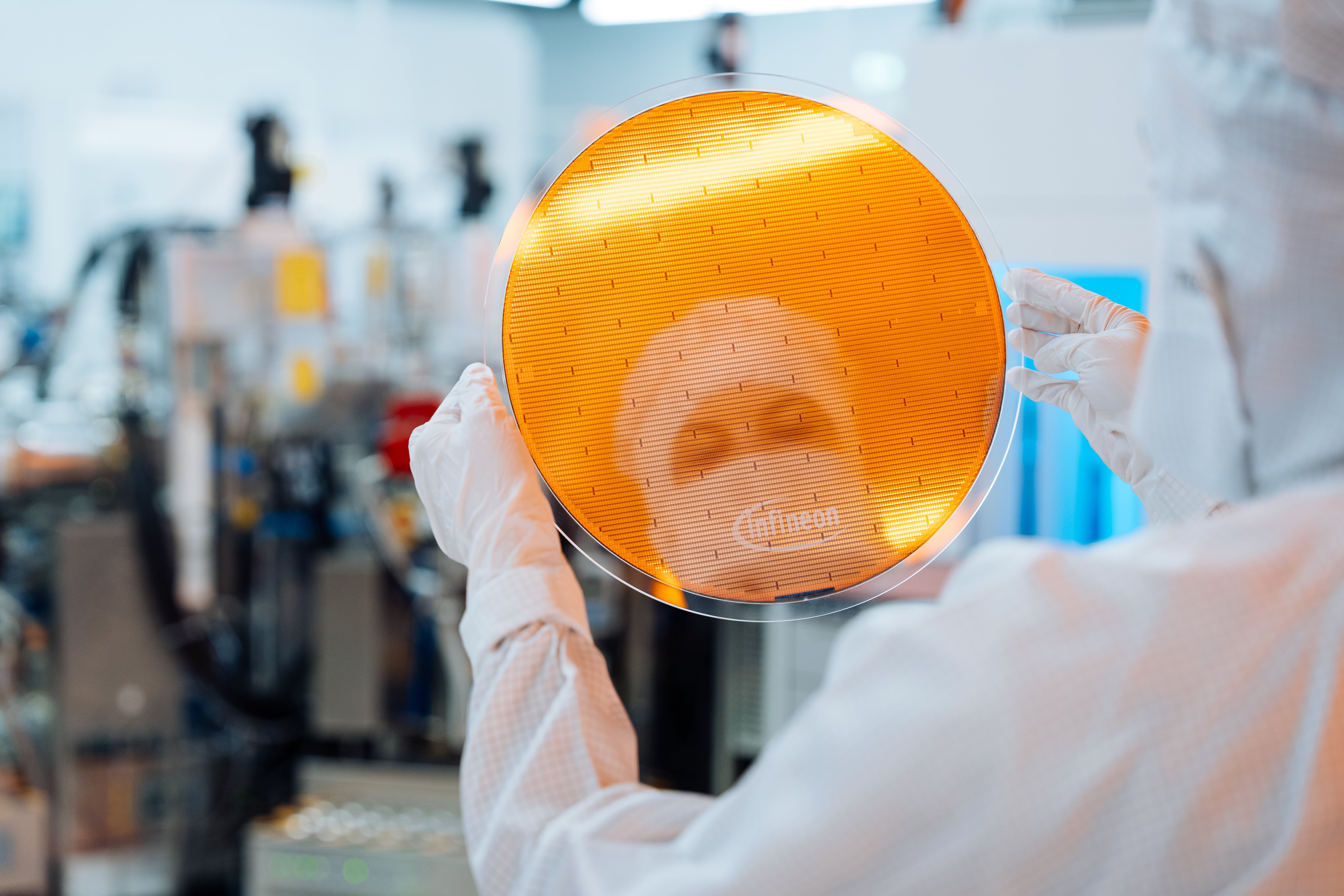
Infineon Technologies AG has unveiled a groundbreaking advancement in the semiconductor industry, revolutionizing performance and efficiency with their development of ultra-thin 300mm silicon power wafers. These wafers, measuring a mere 20 micrometers in thickness, are now officially the world’s thinnest, comparable to the width of a human hair. This feat sets a new benchmark in the semiconductor landscape, offering a host of benefits.
This innovation slashes substrate resistance by 50 percent and reduces power loss by over 15 percent when compared to traditional silicon wafers. Achieving this ultra-thin dimension wasn’t without challenges; Infineon’s engineers had to tackle multiple technical obstacles, such as creating a new wafer-grinding technique for handling the metal stack that anchors the chip on the wafer, which is actually thicker than the wafer itself. They also addressed issues like wafer bowing and separation during back-end assembly, ensuring the wafers are robust enough to be integrated into existing high-volume production lines.
The advanced wafer technology has already been incorporated into Infineon’s Smart Power Stages for DC-DC conversion and is being shipped to customers. Infineon predicts that this energy-efficient design will replace current low-voltage power converter wafers in the next three to four years, paving the way for more efficient electronic devices.
For those interested in witnessing this technological marvel, Infineon will be showcasing the ultra-thin silicon wafer at Electronica 2024 in Munich from November 12-15. This event will offer a closer look at how Infineon’s innovation is set to transform the future of semiconductor technology.


