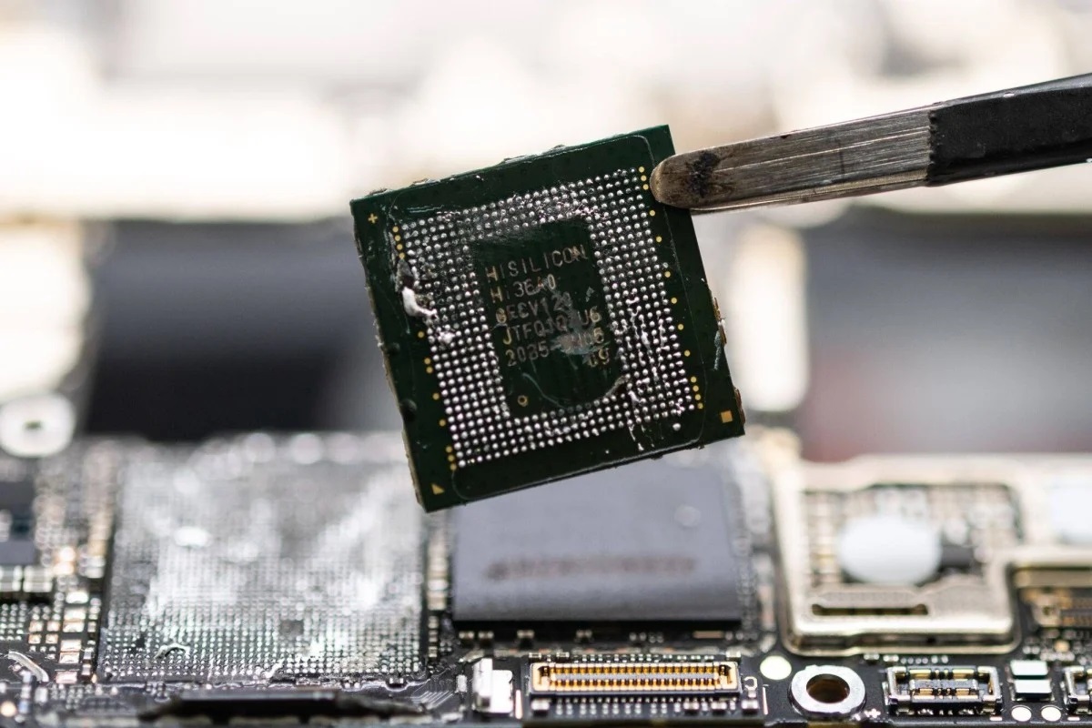
With the imposition of trade sanctions, Huawei has faced significant challenges in developing and manufacturing its Kirin chipsets. Constrained by these limitations, the tech giant has been compelled to depend on its domestic partner, Semiconductor Manufacturing International Corporation (SMIC), China’s top semiconductor company, to propel the advancement of its future chipset generations through sophisticated manufacturing processes.
SMIC has reportedly achieved success in developing a 5nm process, which is expected to be utilized in the upcoming Kirin 9100 chipset, earmarked for the anticipated Mate 70 series. Notably, a move to a more refined manufacturing process is on Huawei’s radar, but a Huawei executive has articulated a different short-term strategy.
During a posted keynote, Zhang Pingan, Huawei’s Executive Director, clarified that the company’s current strategy does not revolve primarily around transitioning to 5nm or 3nm processes. Huawei Central reveals that the focus, instead, is to hone the 7nm process, which is thought to be plagued by low yields and other technical difficulties. The company’s intention is to enhance the chip architecture, thereby addressing deficiencies inherent in the semiconductor design.
Improving the innate capabilities of the chip is considered more critical than fixating on a progression to a finer manufacturing process. Success in refining the architecture could substantially benefit Huawei by allowing it to tackle vulnerabilities within the chip’s design. The cost considerations are palpable: reports have suggested that the production cost for 5nm wafers at SMIC could be comparatively higher—up to 50 percent more than those produced by Taiwan Semiconductor Manufacturing Company (TSMC) using the same node attribute. This cost difference is partially attributed to SMIC’s reliance on older, deep ultraviolet (DUV) lithography equipment instead of the more current extreme ultraviolet (EUV) lithography technology.
EUV lithography tools are essential for efficient production at smaller process nodes like 7nm and below. However, ASML, the sole manufacturer of this sophisticated EUV equipment, is prohibited from supplying these tools to Chinese companies. This condition means that Chinese firms, including SMIC, are potentially hindered from competing effectively against U.S. semiconductor companies.
Despite these obstacles, there is speculation that Huawei and SMIC might have strategies or knowledge that have not been publicized. These could potentially aid them in overcoming their 7nm production woes without the advanced EUV machinery. However, until Huawei and SMSC can gain access to such advanced equipment, the full resolution of the 7nm challenges highlighted by the Huawei executive remains uncertain.
In conclusion, Huawei is taking a careful yet strategic approach, prioritizing the improvement of its 7nm chip yields and resolving existing challenges. Only time will tell whether this method will yield the desired results, allowing the company to eventually shift its focus to 5nm and smaller nodes in the future, despite the current technological and trade constraints.


