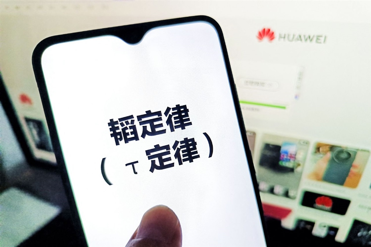
Huawei Pushes Tau Law V2 as a New Post-Moore Strategy for Faster Chips
Huawei is putting forward a new vision for the future of semiconductors, one that moves beyond the traditional race to make transistors smaller. The company’s semiconductor leadership is now promoting a framework called Tau Law V2, a post-Moore roadmap that focuses on reducing time and latency across the entire computing stack.
For decades, the chip industry has relied heavily on Moore’s Law, the idea that packing more transistors into smaller spaces would continue to deliver faster, more efficient processors. But as advanced manufacturing becomes more difficult and expensive, chipmakers are increasingly looking for new ways to improve performance. Huawei’s proposal suggests that the next major gains may come not only from better fabrication processes, but from optimizing how quickly data moves, how efficiently software interacts with hardware, and how much delay can be removed from every stage of computing.
The central idea behind Tau Law V2 is simple: speed is not only about raw transistor density. In modern computing, performance is shaped by the time it takes for data to travel between memory, processors, accelerators, networks, software layers, and applications. By reducing delays throughout that chain, systems can become faster and more efficient even without relying solely on the most advanced chipmaking nodes.
This approach is especially important as the semiconductor industry faces physical limits in miniaturization. Shrinking transistors remains valuable, but it no longer guarantees the same dramatic performance improvements seen in earlier decades. Power consumption, heat, memory bottlenecks, packaging challenges, and software inefficiencies all play a larger role in real-world performance.
Huawei’s time-based framework appears to place greater emphasis on full-system optimization. That means improving chip architecture, memory access, interconnect design, compiler efficiency, workload scheduling, and AI acceleration as part of one broader performance strategy. Instead of treating the processor as an isolated component, Tau Law V2 looks at the entire computing environment.
The company has connected this strategy to its own semiconductor efforts, including Kirin chips used in consumer devices and Ascend accelerators designed for artificial intelligence workloads. Huawei has claimed progress in internal chip production and performance optimization, suggesting that its focus is not limited to hardware manufacturing alone. The broader goal is to make its computing platforms more responsive, efficient, and scalable by cutting wasted time wherever possible.
This shift is particularly relevant for AI computing. Artificial intelligence workloads depend heavily on moving huge amounts of data between memory and processing units. Even powerful accelerators can be slowed down if data transfer, communication, or software coordination introduces delays. A time-focused chip strategy could help improve AI training, inference, and large-scale computing by targeting these bottlenecks directly.
For smartphones, the same principle could improve responsiveness, battery life, app performance, camera processing, and on-device AI features. In cloud and data center environments, reducing latency across processors, accelerators, storage, and networking could lead to better throughput and lower operating costs.
Huawei’s Tau Law V2 also reflects a broader industry trend. As Moore’s Law becomes harder to sustain, companies are exploring alternatives such as advanced packaging, chiplet designs, specialized accelerators, memory-centric computing, and hardware-software co-design. Huawei’s version of this shift puts “time” at the center of the performance equation.
If successful, this strategy could help the company strengthen its position in key areas such as AI chips, mobile processors, cloud infrastructure, and high-performance computing. However, the impact of Tau Law V2 will depend on how effectively Huawei can turn the concept into measurable performance gains across real products.
What makes the proposal notable is that it challenges the industry’s long-standing obsession with transistor scaling. Instead of asking only how small a chip can become, Huawei is asking how much time can be removed from the entire computing process.
As the chip industry enters a more complex post-Moore era, that question may become increasingly important. Faster computing may no longer come from smaller transistors alone, but from smarter systems that reduce every unnecessary delay between data, hardware, software, and the user.