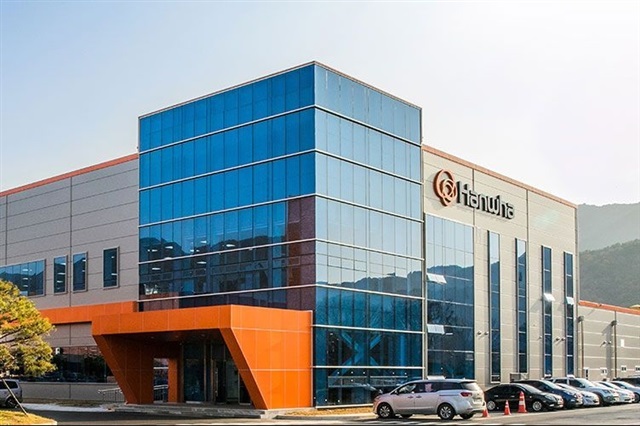
South Korea’s semiconductor equipment specialist Hanwha Semitech is reportedly gearing up for a major move in advanced chip packaging, with plans to supply fan-out panel-level packaging (FO-PLP) equipment in the second half of 2026. The tools are expected to be used for high-volume manufacturing, signaling that FO-PLP is moving closer to mainstream adoption as chipmakers hunt for better performance, efficiency, and cost control.
Fan-out panel-level packaging has become one of the most closely watched packaging technologies because it can help manufacturers produce more chips per panel than traditional wafer-based approaches, potentially improving throughput while reducing packaging costs at scale. As modern processors push higher bandwidth and denser interconnects, packaging is increasingly where big gains are made—especially for AI accelerators, high-performance computing, and advanced networking hardware.
Hanwha Semitech’s reported timeline points to the growing urgency around next-generation packaging equipment. With demand rising for compact, power-efficient chips that can handle intensive workloads, manufacturers are investing more heavily in packaging innovations that support faster data movement and better thermal performance. FO-PLP is often positioned as a strong answer to these needs, enabling high-density designs in thinner, lighter form factors.
The equipment is expected to play a role in mass production tied to a SpaceX-linked chip manufacturing effort, according to reports. While details remain limited, the connection has drawn attention because it suggests a supply chain aligning around high-reliability, high-performance silicon—exactly the kind of chips where advanced packaging can provide a meaningful edge.
If the reported schedule holds, the second half of 2026 could mark an important ramp-up period for panel-level fan-out packaging in production environments. For the semiconductor industry, that’s a notable development: packaging has become a central battleground for performance and cost, and FO-PLP is increasingly viewed as a technology that can help meet soaring compute demand without relying solely on ever-smaller process nodes.
As chip production strategies evolve, moves like this underscore a broader shift—where the future of cutting-edge chips isn’t just about how they’re made, but how they’re packaged, connected, and scaled for real-world volume manufacturing.


