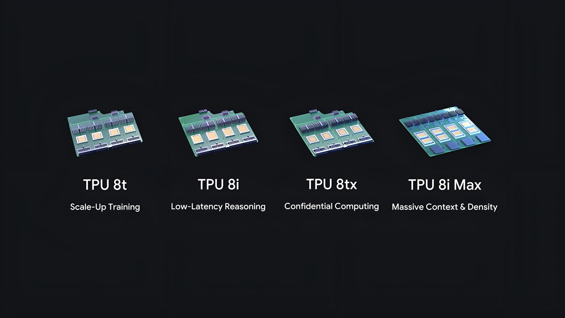
Google expands its TPU v8 lineup with TPU 8tx and TPU 8i Max for secure agentic AI workloads
Google has broadened its TPU v8 family with two new AI accelerator variants designed for the next wave of agentic AI systems. The new TPU 8tx focuses on confidential inference and smaller-scale training, while the TPU 8i Max is built to push past the growing memory limits faced by large AI models, especially those using long context windows and complex multi-step reasoning.
The announcement marks a major expansion of Google’s custom AI silicon strategy. With TPU 8t, TPU 8i, TPU 8tx, and TPU 8i Max now part of the same generation, Google has introduced four TPU variants in a single year, highlighting how quickly AI hardware is evolving to support training, inference, security, and memory-intensive workloads.
The foundation: Google TPU 8t for AI training
The TPU 8t is primarily designed for AI model training. It uses what Google calls a Zebra package, which brings together a central logic chiplet, a dedicated SerDes chiplet, and multiple high-bandwidth memory stacks inside one advanced package.
At the center of the TPU 8t is the TensorCore, the main compute engine responsible for accelerating AI workloads. This block includes a Vector Processing Unit, dedicated vector memory, two Matrix Multiply Units, two eXtended Logic Units, and a Tensor Core System block.
One of the most important features of the TPU 8t is native FP4 support. FP4, or 4-bit floating point, allows the chip to process AI calculations more efficiently, increasing throughput while reducing the power and bandwidth costs associated with moving large amounts of data. With FP4 support, the TPU 8t can deliver up to 12.6 petaFLOPS of FP4 compute per chip.
Google’s design also balances matrix and vector processing so that operations such as softmax can run alongside matrix multiplication. This helps keep the hardware busy and improves utilization, which is critical when training increasingly large AI models.
The TPU 8t also includes two dedicated Sparse cores. These are designed to handle irregular and data-dependent memory access patterns, such as embedding lookups. By offloading these tasks from general compute units, the chip can reduce bottlenecks that often slow down large-scale AI training.
TPU 8t memory and bandwidth
Memory bandwidth is a central part of modern AI chip performance, and the TPU 8t is built with that challenge in mind. A central memory and DMA interconnect links the compute blocks to six HBM3E controllers. These controllers connect to six adjacent 8-hi HBM3E memory stacks within the same package.
Depending on configuration, the TPU 8t offers between 216 GB and 288 GB of high-bandwidth memory per chip. Bandwidth ranges from 6.5 TB/s to 8.6 TB/s, giving the accelerator the data flow required for demanding AI workloads.
The chip also integrates 128 MB of on-die SRAM, allowing frequently used data and parameter layers to remain close to the compute engines. This reduces latency and limits the need to fetch data from farther memory resources.
For scaling across systems, the TPU 8t uses an interconnect module with an ICI router and link stack blocks connected to an external SerDes chiplet. This SerDes chiplet includes 6x224G SerDes octals, enabling very high chip-to-chip data transfer speeds.
Host integration is handled through a PCIe Gen5 x16 interface, with a secondary PCIe Gen2 x1 connection for management through a baseboard management controller. Google also pairs these accelerators with its Arm-based Axion CPUs, which support host-side tasks such as preprocessing and help keep the TPUs supplied with data.
TPU 8i: Google’s inference-focused AI accelerator
While the TPU 8t is aimed at training, the TPU 8i is built for inference. It also uses the Zebra package approach, splitting the design between a central logic chiplet and a dedicated SerDes chiplet.
The TPU 8i contains two TensorCores, making it especially compute-dense for inference workloads. Each TensorCore includes a Vector Processing Unit, vector memory, two Matrix Multiply Units, two eXtended Logic Units, and a Tensor Core System block.
This dual-core layout enables the TPU 8i to reach up to 10.1 petaFLOPS of peak FP4 compute performance. That makes it well suited for serving AI models efficiently, especially as demand grows for fast, low-latency generative AI responses.
The memory system is also designed around inference efficiency. The TPU 8i uses two memory and DMA interconnect modules on the logic chiplet. Each routes data to four HBM3 controllers, with each controller connected to an 8-hi HBM3E memory stack. In total, the TPU 8i integrates eight HBM3E stacks directly onto the package.
Each TPU 8i chip includes 288 GB of HBM3E with bandwidth of up to 8.6 TB/s. It also includes 384 MB of on-chip SRAM, which can be used for active key-value cache. This is especially important for AI inference because KV cache management can become a major bottleneck in large language models, particularly during long conversations or extended context processing.
Google also replaces traditional x86 host processors in TPU 8i servers with its custom Arm-based Axion processors. These CPUs use DDR5 memory and handle system-level functions such as data preprocessing and host management.
For networking, the TPU 8i includes an ICI module with an ICI router, a 6x link stack, and an SC-CAE block. This connects to the external SerDes chiplet, which contains 6x200G SerDes octals and a Physical Coding Sublayer for managing large amounts of off-chip data transfer.
TPU 8tx: confidential computing for agentic AI
The newly introduced TPU 8tx is a modified version of the TPU 8t. Its main focus is confidential inference, secure AI processing, and agentic workloads.
Agentic AI systems are designed to perform multi-step tasks, make decisions, use tools, and operate with more autonomy than traditional chatbots. These workloads can involve sensitive data, proprietary model weights, and real-time decision-making, which makes security increasingly important.
To address this, the TPU 8tx combines TPU 8t silicon with custom AMD CPU hosts and adds hardware-level confidential computing. This helps protect both data and model weights while they are being processed, rather than only when they are stored or transmitted.
Google says the TPU 8tx also adopts the Boardfly network developed for the TPU 8i. With these changes, the TPU 8tx can deliver up to twice the performance of the TPU 8t while maintaining a near-zero performance penalty for its enhanced security features.
That combination is significant. Confidential computing often comes with some performance trade-off, but Google is positioning TPU 8tx as a secure AI accelerator that can protect sensitive workloads without slowing them down in a meaningful way.
TPU 8i Max: built to break through the AI memory wall
The second new chip, TPU 8i Max, is designed to address one of the biggest challenges in AI today: the memory wall.
As AI models grow more capable, they require more memory bandwidth, more on-chip cache, and more capacity for long context windows. Agentic AI workloads can push this even further because they may need to process large amounts of information across multiple steps, tools, documents, and interactions.
The TPU 8i Max is based on a dual-chip package that combines two TPU 8i chips. According to Google, this gives the TPU 8i Max twice the compute, twice the SRAM, and twice the HBM bandwidth of a standard TPU 8i.
Because the TPU 8i Max fits into roughly the same rack footprint as the TPU 8i, Google effectively doubles compute density without requiring a major increase in physical infrastructure. That matters for data centers where power, cooling, rack space, and networking capacity are all under pressure.
The TPU 8i Max includes 768 MB of SRAM, a major increase that should help with workloads involving key-value cache and long-context inference. Google has not confirmed the total amount of HBM available on the TPU 8i Max, but the dual-chip design suggests that memory bandwidth and capacity are core parts of its value.
Why Google’s TPU v8 expansion matters
Google’s latest TPU v8 additions show how AI accelerator design is becoming more specialized. Instead of building one chip for every workload, Google is dividing its TPU family around specific needs.
The TPU 8t targets training. The TPU 8i focuses on inference. The TPU 8tx adds confidential computing for secure agentic AI. The TPU 8i Max increases compute density and memory resources for long-context and memory-heavy workloads.
This reflects a broader shift in AI infrastructure. The next generation of AI systems will not only need more raw compute. They will also need faster memory, larger on-chip cache, better networking, stronger data protection, and tighter host integration.
For enterprises, cloud providers, and AI developers, chips such as the TPU 8tx and TPU 8i Max point toward a future where secure AI inference and memory-rich agentic workloads become mainstream. Google is positioning its TPU v8 family to handle that future with dedicated silicon built for performance, efficiency, and security.