DRAM Giants Turn to 3D Stacking as Traditional HBM Nears Its Limit
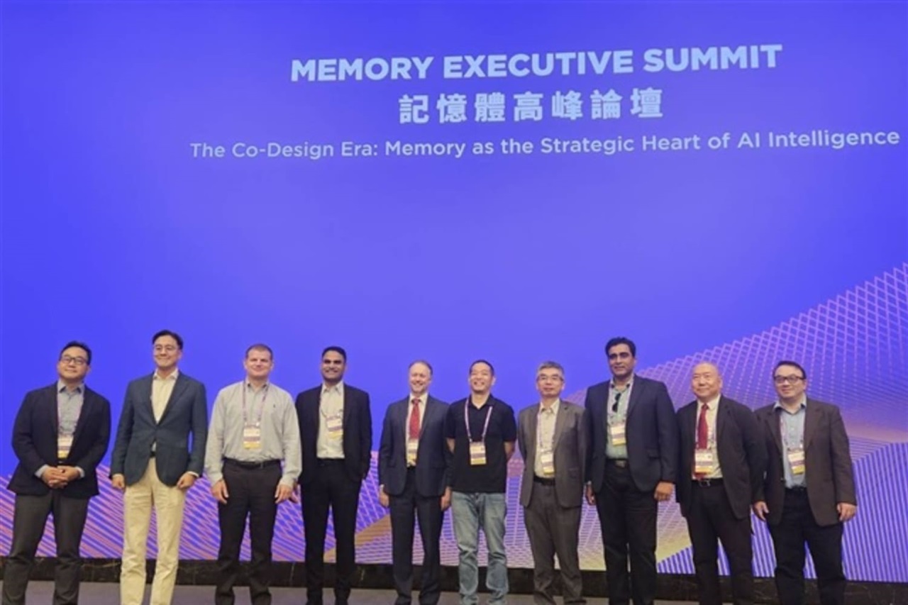
The memory industry is preparing for a major shift as demand for faster, more efficient data processing continues to surge. At Semicon Taiwan 2026, leaders from Samsung Electronics, SK Hynix, and Micron shared a common view: conventional 2.5D high-bandwidth memory, widely known as HBM, is getting close to its practical performance ceiling.
For years, 2.5D HBM designs have relied on interposers to connect memory stacks with processors. This approach has helped power the rapid growth of AI accelerators, data centers, high-performance computing systems, and advanced graphics hardware. However, as workloads become more complex and data movement increases, the limits of current packaging technology are becoming harder to ignore.
The next major step is 3D vertical stacking.
By moving toward true 3D architectures, memory makers aim to reduce the distance that data must travel between components. Shorter transmission paths can help lower power consumption, improve bandwidth, and increase overall efficiency. This is especially important for artificial intelligence and machine learning systems, where memory speed and energy efficiency are now just as critical as raw computing power.
Wafer-level bonding is expected to play a key role in this transition. Instead of depending mainly on traditional interposer-based layouts, manufacturers are looking at advanced bonding methods that allow memory layers and logic components to be integrated more closely. This tighter integration could help overcome the so-called “memory wall,” a long-standing challenge where processors become faster than memory systems can efficiently supply data.
The push toward 3D stacked DRAM reflects a broader change in the semiconductor industry. Performance gains are no longer coming only from smaller process nodes. Packaging, stacking, and interconnect technologies are becoming essential tools for delivering the next generation of computing power.
For Samsung Electronics, SK Hynix, and Micron, the move beyond 2.5D HBM is not just a technical upgrade. It is a strategic response to the explosive growth of AI infrastructure, cloud computing, and data-heavy applications. As demand for high-bandwidth, low-power memory accelerates, 3D stacking could become the foundation of future memory innovation.
If successful, this transition may reshape the design of next-generation AI chips, servers, supercomputers, and advanced consumer electronics. The era of traditional HBM is not ending overnight, but the industry’s direction is becoming clear: the future of memory is moving upward, layer by layer.