Intel Reportedly Teams Up With AU Optronics to Advance Co-Packaged Optics and High-Density Chip Packaging
Intel is reportedly accelerating its advanced chip packaging strategy through a potential collaboration with AU Optronics, a Taiwanese display and optoelectronics company known for its Micro LED expertise. The partnership is said to focus on co-packaged optics, Micro LED substrates, glass substrates, and highly integrated chip designs built for next-generation computing.
The move comes as the semiconductor industry looks for new ways to improve performance beyond traditional transistor scaling. With Moore’s Law becoming harder to sustain, advanced packaging has become one of the most important paths forward. Instead of relying only on smaller process nodes, companies are now using sophisticated packaging methods to combine multiple chips, optical components, and interconnect technologies into a single high-performance system.
This is especially important for artificial intelligence, data centers, high-performance computing, and networking hardware, where bandwidth, power efficiency, and thermal control are becoming major challenges. Co-packaged optics, often shortened to CPO, is viewed as a key technology for solving some of these bottlenecks by bringing optical communication closer to the processor or accelerator.
According to industry reports, Intel and AU Optronics may work together on advanced integration solutions involving Micro LED substrates and glass-based packaging. AU Optronics has built strong experience in Micro LED technology, optical interconnects, redistribution layers, and glass substrate development. These areas appear to align closely with Intel’s own work in advanced packaging.
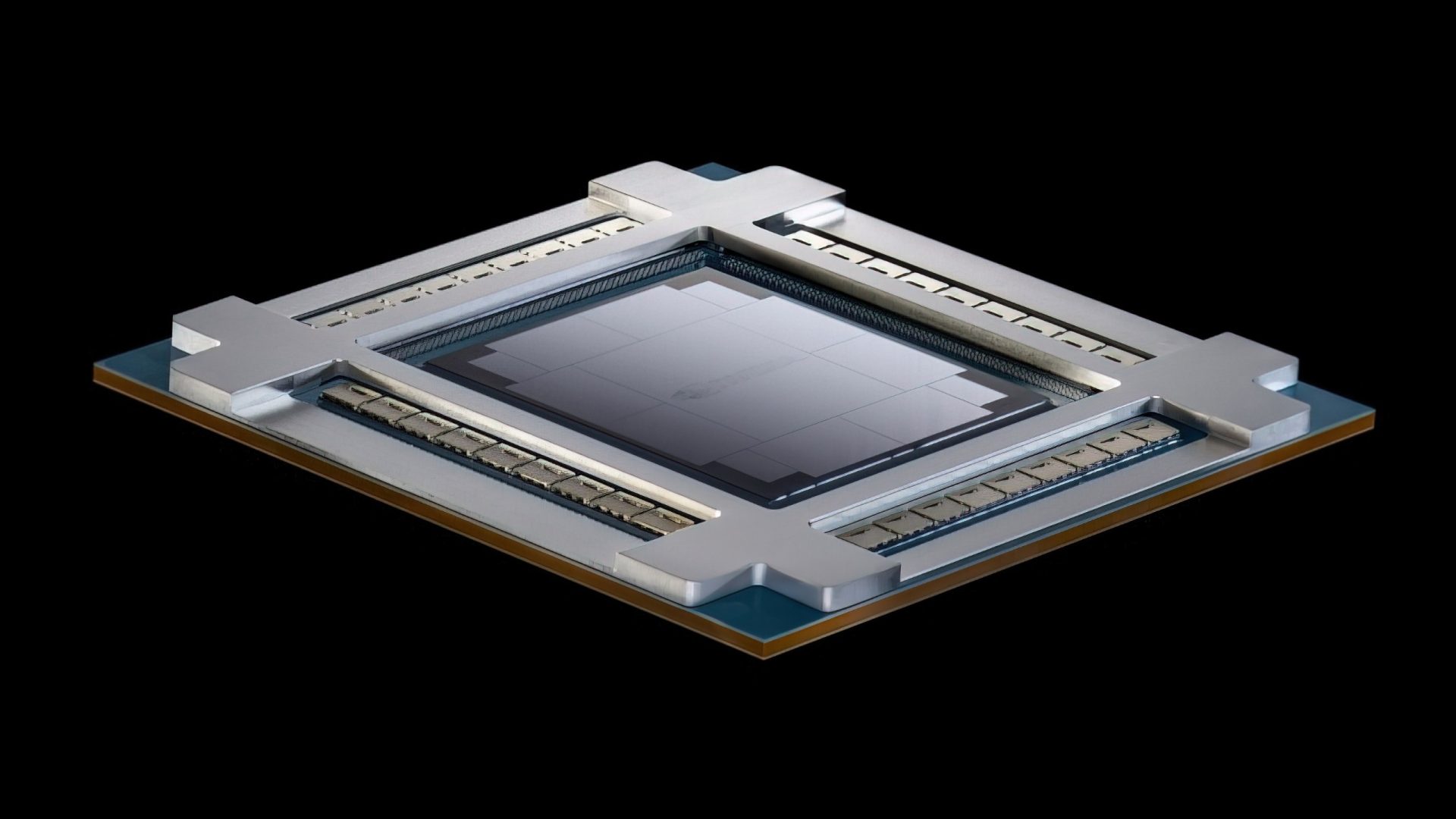
Intel has already made significant progress with its Embedded Multi-Die Interconnect Bridge technology, better known as EMIB. This packaging approach allows multiple chiplets to communicate at high speeds inside a package without requiring a large silicon interposer. Intel has also been investing heavily in glass substrate technology, which could play an important role in future chip packaging because of its stability, scalability, and potential for high-density interconnects.
One of the more interesting details surrounding Intel’s recent activity is a U.S. patent involving integrated circuits packaged on Micro LED substrates. The patent describes semiconductor chip sections embedded within a glass substrate that uses through-glass vias, or TGVs. This differs from more traditional through-silicon vias, or TSVs, and could open the door to new types of heterogeneous integration.
Heterogeneous integration is becoming increasingly important because modern processors are no longer just single monolithic chips. Instead, they often combine compute dies, memory, I/O components, optical interfaces, and specialized accelerators. By integrating these elements more closely, chipmakers can improve speed, reduce latency, and lower power consumption.
For co-packaged optics, this type of integration is especially valuable. Data centers and AI systems require massive amounts of data to move between processors, memory, and networking equipment. Traditional electrical interconnects face limits in bandwidth and efficiency, while optical interconnects can deliver faster data transmission over longer distances with improved energy efficiency. Bringing optics directly into the package could help reduce signal loss and improve system-level performance.
AU Optronics could be a strong partner in this area because of its existing Micro LED and optoelectronics background. Micro LED technology is often associated with advanced displays, but its manufacturing techniques and substrate knowledge may also support next-generation optical and semiconductor packaging. Combined with Intel’s chip packaging experience, the collaboration could help create new solutions for AI accelerators, high-density computing chips, and advanced networking hardware.
Reports suggest that AU Optronics has already been expanding into advanced packaging and glass substrate technologies. Its ecosystem reportedly includes Micro LED CPO development, redistribution layer processes, optical interconnect work, and glass substrate capabilities. These strengths could complement Intel’s efforts as it pushes deeper into chiplet-based designs and future packaging platforms.
Neither company has officially confirmed the partnership. Intel has reportedly declined to comment, while AU Optronics leadership has previously acknowledged the company’s growing involvement in advanced packaging and glass substrates. Even without formal confirmation, the technical overlap between the two companies makes the rumored collaboration appear strategically sensible.
If the partnership moves forward, it could strengthen Intel’s position in the race for next-generation semiconductor packaging. The company is competing in an industry where packaging is becoming just as important as transistor design. As AI workloads grow and data center infrastructure demands faster interconnects, technologies such as glass substrates, Micro LED integration, TGVs, and co-packaged optics may become central to future chip development.
The bigger picture is clear: the semiconductor industry is entering an era where performance gains will come from smarter integration, not just smaller chips. Intel’s reported work with AU Optronics could be part of that transition, combining advanced packaging with optical communication to support the next wave of high-density computing.
If successful, this collaboration could help shape future AI hardware, data center processors, and optical interconnect platforms, giving both companies a stronger role in one of the most important technology shifts in modern computing.