AMD is gearing up to introduce its Krackan Point APUs, designed as a mainstream Ryzen AI option, featuring support for faster LPDDR5X memory. These new chips, part of AMD’s aggressive expansion in the mobile CPU market, will follow the Phoenix and Hawk Point series and sit alongside the upcoming Strix series.
Krackan Point APUs will be built on a monolithic design integrating Zen 5 and Zen 5c cores for energy-efficient performance. The integrated GPU will feature RDNA 3.5 graphics architecture. Recent information from Lenovo China’s Product Manager indicates that Krackan Point APUs will support up to LPDDR5X-8000 memory, an improvement over the initially suggested 7,500 MT/s. This enhancement puts AMD in a competitive stance, especially since Intel’s upcoming Lunar Lake CPUs will support LPDDR5-8533 memory.
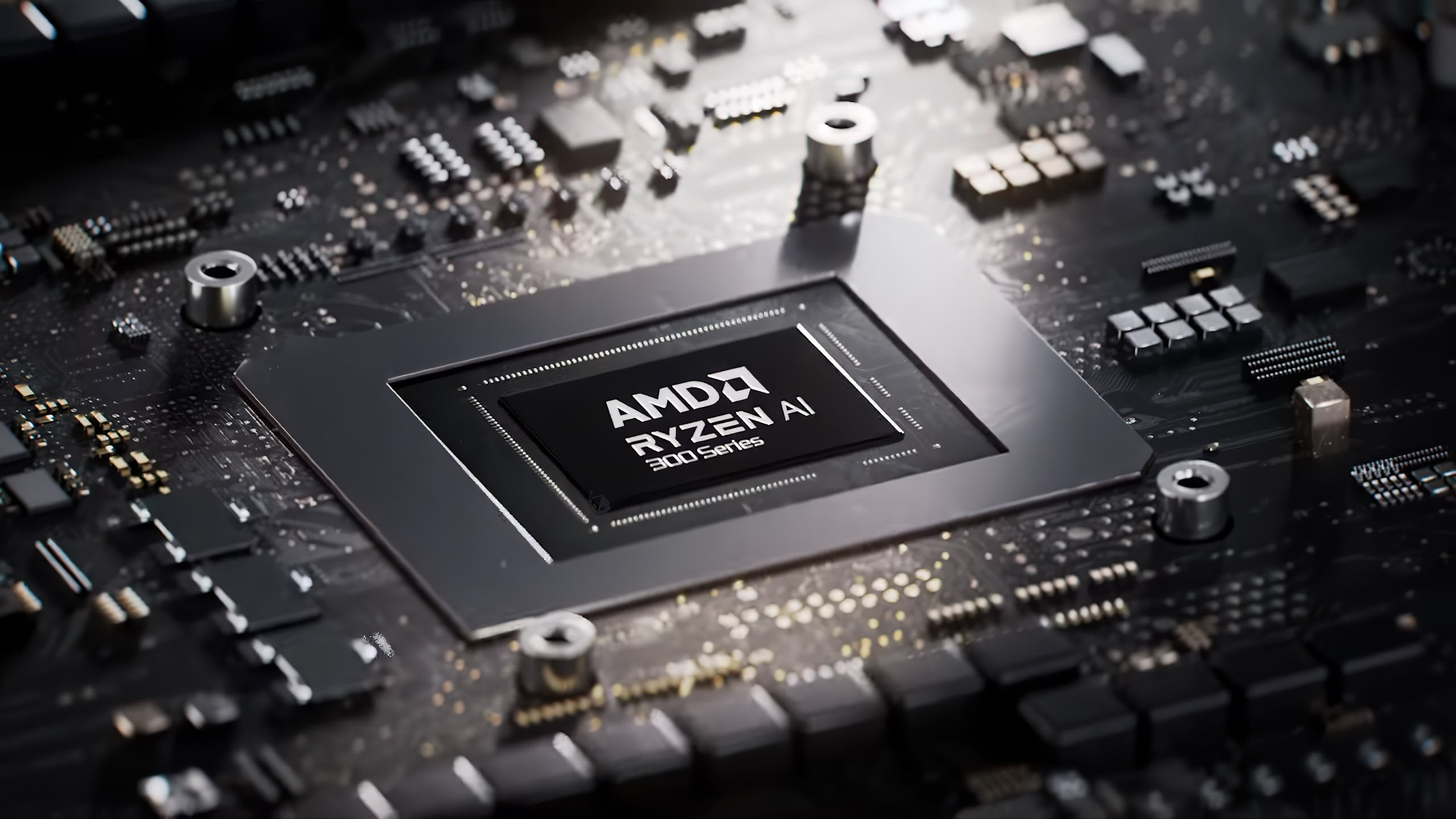
Key features expected in the AMD Ryzen AI HX Krackan Point include:
Zen 5 Monolithic Design
Up to 8 cores (4 Zen 5 + 4 Zen 5C)
16 MB of shared L3 cache
8 RDNA 3.5 Compute Units
Support for LPDDR5X-8000 memory
Integrated XDNA 2 Engine
Up to 50 AI TOPS
1H 2025 launch timeframe
FP8 platform (15W-45W TDP range)
The Krackan Point APUs are anticipated to bring significant improvements over the Hawk Point series, especially for mainstream users focusing on AI-enhanced applications and mobile computing. Alongside the Strix Halo series, these next-generation mobile SoCs are expected to cover a wide range of market segments. Both Krackan Point and Strix Halo are slated for release around CES 2025.
AMD has an extensive roadmap for its Ryzen Mobility CPUs, with various families planned, each targeting specific market needs. These include CPUs from the Dragon Range, Phoenix, Rembrandt, and more, all expected to deliver incremental improvements and innovations in mobile computing over the next few years.