AMD is preparing a major leap for its Instinct MI500 AI accelerators, and a key part of that plan includes a new co-packaged optics approach built with help from GlobalFoundries. The goal is simple: deliver faster, more efficient data movement inside next-generation AI systems where traditional copper connections are increasingly becoming a bottleneck.
Co-Packaged Optics, often shortened to CPO and closely tied to silicon photonics, is emerging as a crucial technology for future AI “factories.” Instead of relying heavily on electrical signaling over copper, CPO uses light to move data. By placing optical components directly alongside high-performance accelerators like GPUs, CPO can reduce interconnect latency and enable extremely high-bandwidth links between compute devices such as CPUs and GPUs. As AI clusters grow larger and more power-hungry, these improvements can translate into better scalability and lower overall energy costs for moving data around.
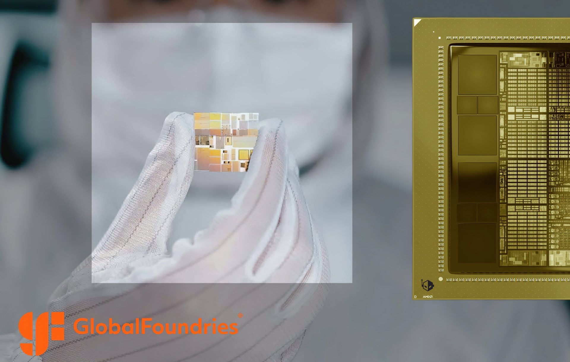
For AMD’s next-gen Instinct MI500 lineup, the latest information points to an MRM-based co-packaged optics solution. In this setup, the Photonic Integrated Circuits (PICs) are expected to be manufactured by GlobalFoundries, while ASE is set to handle the advanced packaging work. AMD has been building toward this moment for a while; its acquisition of photonics specialist Enosemi was widely seen as a move to accelerate development of in-house optical technology and bring CPO innovations to market faster.
The broader AI GPU industry is moving in the same direction. NVIDIA is also believed to be developing its own CPO-related photonic integrated circuits for its Vera Rubin accelerator platform, with manufacturing and packaging spread across multiple partners. In addition, Rubin Ultra is reportedly expected to prioritize CPO over Near-Package Optics (NPO), signaling that fully integrated optical interconnects are becoming the preferred option as performance demands rise. Looking further ahead, NVIDIA is rumored to be pushing even harder into co-packaged optics with its Feynman generation, potentially moving beyond NPO entirely.
On the silicon side, AMD has already confirmed that the Instinct MI500 series will be produced using an advanced 2nm-class process at TSMC. The MI400 series is also tied to 2nm technology, but MI500 is expected to use a more advanced variation with additional enhancements. MI500 is set to introduce AMD’s CDNA 6 architecture (with MI400 using CDNA 5) and adopt HBM4E memory. That memory upgrade matters: HBM4E is expected to deliver even higher speeds and bandwidth than what’s projected for HBM4-based MI400 accelerators, which are cited around 19.6TB/s. Another notable detail for AMD watchers is that the Instinct naming and architecture branding appears to be staying on the CDNA track rather than switching to a UDNA naming approach.
All of this feeds into AMD’s bigger promise: a dramatic jump in AI performance with Instinct MI500. The company has outlined an aggressive trajectory targeting more than a 1000x improvement in AI performance over a four-year span, a necessary pace as hyperscalers and enterprises continue to expand their AI infrastructure at breakneck speed.
AMD’s Instinct MI500 accelerators are currently expected to launch in 2027, and if co-packaged optics arrives as planned, MI500 could be one of the first major AMD platforms where silicon photonics becomes a core piece of the scaling strategy—not just a future experiment.