Advanced Packaging Moves Toward Full System Integration as AI Reshapes the Semiconductor Industry
Advanced semiconductor packaging is quickly becoming one of the most important battlegrounds in the global chip industry. As artificial intelligence workloads demand faster processing, higher bandwidth, lower latency, and better energy efficiency, chipmakers and research organizations are looking beyond traditional methods of placing chips together. The future is increasingly focused on system-level integration, where multiple technologies work as one highly optimized computing platform.
At the Innovate Together 2026 conference in Singapore on September 25, industry leaders and researchers from A*STAR’s Institute of Microelectronics, KLA, ASM International, the National University of Singapore, the SHINE Centre, and ASMPT explored how advanced packaging is entering a new phase. The discussion highlighted that packaging is no longer simply the final step in semiconductor manufacturing. It is now a core part of chip design, performance scaling, and AI hardware innovation.
One of the biggest themes was the growing importance of optical interconnects. As AI systems become larger and more complex, traditional electrical connections can struggle with power consumption and data transfer limits. Optical interconnect technology offers a potential path toward faster communication between chips while reducing energy loss. This could be especially valuable for data centers, AI accelerators, high-performance computing systems, and next-generation networking infrastructure.
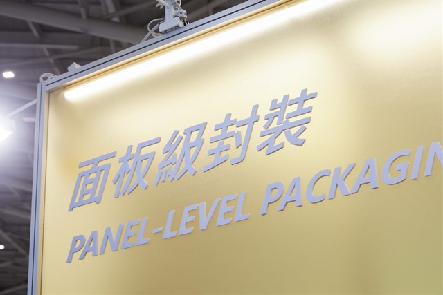
Panel-level packaging was another major focus. Compared with conventional wafer-level approaches, panel-level packaging may allow manufacturers to process more chips at once, improving production efficiency and potentially lowering costs. As demand for AI chips continues to rise, scalable packaging methods could become essential for meeting global supply needs.
Speakers also emphasized that the industry must address workforce development. Advanced packaging requires expertise across materials science, chip design, manufacturing equipment, photonics, testing, and system architecture. As packaging grows more sophisticated, companies and research institutions will need to train a new generation of engineers capable of working across these disciplines.
The shift toward system integration reflects a broader change in the semiconductor sector. For decades, much of chip performance growth came from shrinking transistors. Today, while transistor scaling remains important, the industry is increasingly relying on advanced packaging to deliver performance gains. By combining multiple chips, memory, sensors, and communication technologies into tightly integrated systems, companies can build more powerful and efficient processors for AI and other demanding applications.
Singapore’s role in this discussion is also significant. With its strong research ecosystem, semiconductor manufacturing presence, and partnerships between universities, public research agencies, and global technology firms, the country is positioning itself as an important hub for advanced packaging innovation.
As AI continues to transform computing, advanced packaging will play a central role in determining how future chips are built. Optical interconnects, panel-level manufacturing, and skilled talent development are no longer optional areas of research. They are becoming critical building blocks for the next era of semiconductor technology.