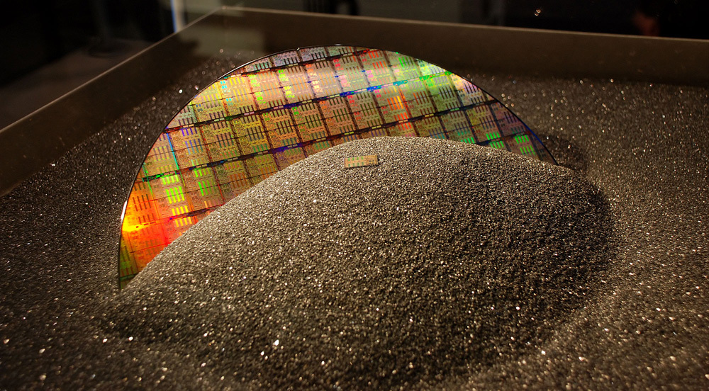
TSMC’s A14 process is moving faster than expected, and the early signs point to a major leap beyond today’s cutting-edge nodes. The company says A14 development is progressing smoothly with yield performance ahead of schedule, setting the stage for one of the most consequential angstrom-era releases on its roadmap.
Positioned as a successor to the 2nm N2 family, A14 is expected to deliver up to 15% higher speed at the same power or up to 30% better power efficiency compared to N2. TSMC plans to reach these gains using second‑generation GAAFET nanosheet transistors and a new NanoFlex Pro standard cell architecture, which together target up to a 20% boost in logic density versus N2. In plain terms, A14 aims to pack more performance into less power and space—exactly what the next wave of AI, mobile, and high‑performance computing products needs.
The update arrives as much of the industry grapples with ramping current 3nm-class technologies. By contrast, TSMC is already signaling confident progress on nodes well beyond 2nm, reinforcing the company’s manufacturing lead. Alongside A14, the roadmap also highlights A16, which integrates nanosheet transistors with Super Power Rail and novel backside contacts to push logic density and efficiency even further.
For device makers, the implications are significant. If A14 lands as projected, it could unlock faster silicon with longer battery life in phones and laptops, while data center and AI accelerator designs benefit from better performance-per-watt and higher transistor budgets. It’s no surprise that top customers across mobile and high‑performance computing are expected to line up for early access.
TSMC currently anticipates A14 entering production in 2028. As design kits mature and partners begin taping out chips, expect A14 to become a cornerstone node for next‑generation processors spanning consumer electronics, PCs, and cloud infrastructure.


 and A12 (1.2nm) for 2029, Holding Off on ASML’s Most Expensive EUV Machines—for Now")


