AMD’s next wave of processors built on the Zen 6 architecture is shaping up to be one of the most meaningful upgrades the company has delivered in years, and the latest details about the core complex die (CCD) help explain why. Even though Zen 6 is expected to keep the CCD at roughly the same physical size as recent generations, it’s reportedly packing far more compute resources thanks to TSMC’s cutting-edge N2 (2nm-class) process technology.
According to information shared by leaker HXL (@9550pro), AMD’s Zen 6 CCD is estimated at around 76mm². That’s notably close to recent Zen CCD sizes, despite a major jump in what’s inside. For context, recent mainstream CCDs have looked like this:
Zen 2 CCD (TSMC N7): ~77mm²
Zen 3 CCD (TSMC N7): ~83mm²
Zen 4 CCD (TSMC N5): ~72mm²
Zen 5 CCD (TSMC N4): ~71mm²
Zen 6 CCD (TSMC N2): ~76mm²
The key takeaway is density. Zen 6 is expected to deliver a sizable increase in cores and cache without a big increase in die area. If the 76mm² figure holds, Zen 6 would be only about 5–7% larger than Zen 4 and Zen 5 CCDs, yet it’s rumored to bring a massive internal upgrade.
12 cores and 48MB L3 cache per CCD, a big jump from the 8-core, 32MB L3 layout used by recent generations. That translates into about a 50% increase in both core count and L3 cache per CCD, which could have major implications for multi-threaded performance, gaming consistency, and content creation workloads that thrive on cache capacity.
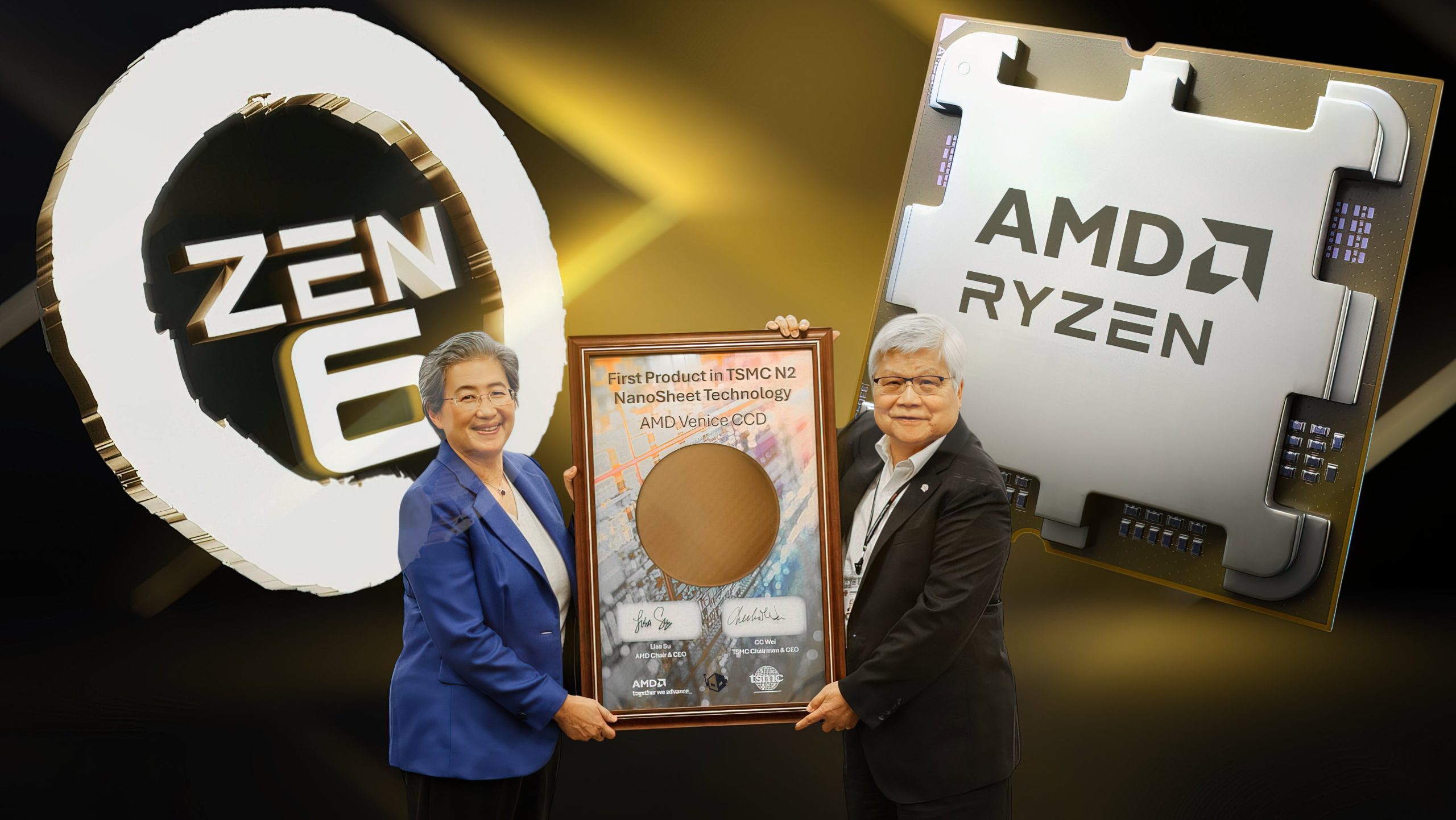
The manufacturing story matters here, too. AMD has already confirmed that EPYC Venice, its future server lineup built on Zen 6, will be the first AMD product made on TSMC’s N2 nanosheet technology. Additional reports suggest AMD may use an enhanced N2P node across much of the Zen 6 family, while the I/O die (IOD) could use N3P. It’s also been suggested that some entry-level chips may continue to rely on N3P, likely to keep costs under control for budget-focused SKUs.
What this could mean for Ryzen Zen 6 desktop CPUs is a more substantial jump than a typical year-to-year refresh. Expectations being discussed include a double-digit IPC (instructions per clock) uplift, higher clock speeds thanks to the better process node, and higher cache capacity. There’s also talk of higher DDR5 memory speed support, a dual IMC design while keeping a dual-channel configuration, and similar overall power targets—suggesting AMD may aim to boost performance without dramatically raising TDPs.
One of the most exciting aspects is how this improved density could scale. Alongside “standard” Zen 6 CCDs, there’s also discussion of a denser variant often referred to as Zen 6C. In that scenario, the die reportedly grows to around 156mm² but could pack as many as 32 cores and 128MB of L3 cache per CCD, which would be an enormous leap for throughput-heavy server and workstation use cases.
Beyond raw cores and cache, Zen 6 is also expected to benefit from continued improvements to AMD’s 3D V-Cache lineup, with rumors pointing toward a third-generation evolution of the stacked-cache approach that has already proven highly effective in gaming and mixed workloads.
If current timelines hold, the first Zen 6-based products—including EPYC Venice and the next-generation Ryzen family—are expected to arrive in the second half of this year. With a near last-gen die size but a much higher core-and-cache payload, Zen 6 could end up being one of the most impactful Ryzen and EPYC updates in recent memory.