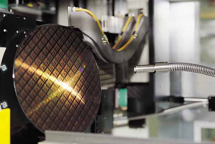
In a frontier-pushing effort to meet the exponential demand for computational power, especially within the AI market, TSMC is experimenting with a revolutionary approach in semiconductor manufacturing: the use of rectangular substrates in advanced chip packaging. This innovative step deviates from the longstanding tradition of circular wafers and has the potential to significantly enhance wafer area utilization.
The adoption of rectangular substrates offers a considerable advantage over existing designs. By shifting to a panel-like substrate with dimensions reported to be around 510 millimeters by 515 millimeters, TSMC is effectively tripling the available space for chip placement. This transition not only raises the bar for manufacturing efficiency but propels the process forward, minimizing wastage of semiconductor material due to the reduced unused space on wafers.
However, the path to implementing these rectangular substrates is riddled with challenges. It demands advanced capabilities in chip stacking, assembly techniques, and a more intricate manufacturing process overall. Currently, these complexities present a considerable barrier to immediate integration within TSMC’s operations. Given the pace at which the AI industry is progressing, though, it’s likely that a shift in industry standards will eventually necessitate the adoption of such innovative approaches.
Analysts recognize that moving to rectangular substrates would demand a comprehensive revamping of manufacturing facilities. Upgrades would be essential throughout the production process, including the addition of new robotic arms and automated material handling systems designed to accommodate the different substrate shapes. A transition of this magnitude is regarded as a long-term endeavor, with a time frame that extends to five or ten years into the future.
TSMC’s strong financial foundation and its established relationships with heavyweight clients like NVIDIA, Amazon, AMD, and Google, position the company advantageously for such an undertaking. Although the changeover to rectangular substrates may entail significant investments, TSMC’s robust economic standing suggests that the need to unlock this next level of efficiency and capability could accommodate such an ambitious move.
For the moment, rectangular substrates remain conceptual and their realization will involve more than just fiscal considerations. If successful, TSMC’s new packaging technique could redefine semiconductor manufacturing and provide the much-needed impetus to AI technologies, propelling them forward with increased performance and greater efficiency.


