Optical communication is entering a major transition, moving away from traditional pluggable optics and toward co-packaged optics (CPO) designs. Instead of keeping optical modules separate and connected through standard plugs, CPO places optical engines much closer to switching silicon. The result is a path toward faster data movement, improved power efficiency, and better scalability—exactly what data centers and AI-driven networks are demanding as bandwidth requirements surge.
At the same time, semiconductor packaging is evolving just as quickly. Advanced packaging, once focused heavily on wafer-level processes, is now expanding into panel-level approaches. One of the most talked-about developments is fan-out panel-level packaging (FOPLP), which takes the fan-out concept used in advanced chip packaging and applies it on large rectangular panels rather than round wafers. Because panels can offer more usable area and improved manufacturing economics at scale, FOPLP is increasingly viewed as a practical option for next-generation high-density packaging.
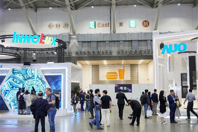
This shift is opening the door for new players and new partnerships—especially among display and panel manufacturing specialists. As packaging needs become more similar to high-precision panel processing, Taiwan’s major panel makers are increasingly positioned to participate in semiconductor packaging opportunities, including CPO-related production flows that demand tight alignment, fine patterning, and stable high-volume manufacturing.
The broader message is clear: the future of optical connectivity and advanced chip packaging is converging. CPO architecture is pushing optics and compute closer together, while panel-level packaging like FOPLP is pushing the industry toward new ways of building and scaling advanced packages. With AI infrastructure, cloud services, and high-speed networking accelerating worldwide, these technologies are shaping up to be key building blocks for next-generation data centers and communication platforms.