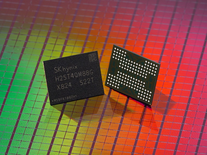
SK Hynix installs first High-NA EUV tool for volume DRAM at M16, accelerating next‑gen memory
SK Hynix has completed assembly of ASML’s TWINSCAN EXE:5200B High-NA EUV lithography system at its M16 fab in Icheon, South Korea—the first High-NA EUV tool set up at a customer site with mass production in mind. Company leaders and ASML representatives marked the milestone on site, highlighting its role in speeding next-generation DRAM development, reinforcing domestic leadership in AI memory, and strengthening supply-chain resilience through deep partner collaboration.
Why it matters: High-NA EUV raises the numerical aperture by about 40 percent versus today’s Low-NA systems, enabling features roughly 1.7 times smaller and delivering around 2.9 times higher transistor density in a single exposure. The EXE:5200B targets an impressive 8 nm resolution, a notable leap from the ~13 nm resolution typical of Low-NA EUV. In practical terms, that means denser, more power-efficient DRAM with better scaling headroom—exactly what’s needed for AI, high-performance computing, and data center workloads.
In the near term, SK Hynix plans to use the tool to rapidly prototype advanced DRAM structures, including capacitor trenches, bitlines, and wordlines, to accelerate node development. As the technology matures, the company also intends to streamline EUV process flows to enhance cost competitiveness and improve throughput and yields.
The move places SK Hynix ahead of rivals still relying on Low-NA EUV lithography, offering a potential advantage in delivering higher-density DRAM sooner. While ASML previously deployed pre-production High-NA systems, such as the NXE:5000 series at Intel’s D1X, SK Hynix’s installation is the first EXE:5200B assembled at a fab designed for volume output. It marks a meaningful step from pilot to practical production readiness.
SK Hynix has been expanding EUV use in DRAM since 2021, and this installation represents the next phase of its scaling roadmap. By embracing High-NA EUV early, the company aims to de-risk the industry’s broader transition expected in the 2030s, gain valuable learning cycles, and bring next-gen DRAM to market faster with higher density and better cost structure.
Bottom line: High-NA EUV at M16 opens a new chapter for SK Hynix’s DRAM manufacturing. Expect faster development, improved density, and stronger positioning in AI-focused memory as the company builds momentum toward future nodes.