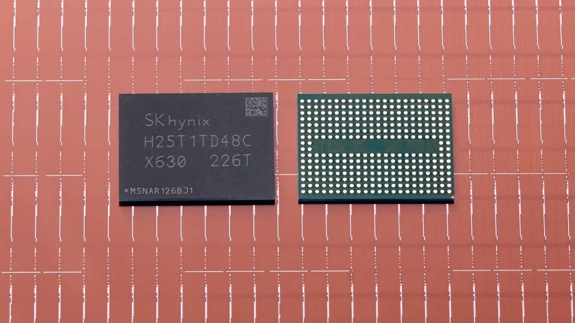
SK Hynix is preparing a major leap in NAND flash technology as it moves toward mass production of its 375-layer NAND solution, expected by the end of 2026. The new memory could bring higher storage capacities, improved performance, and stronger efficiency to future SSDs, smartphones, data centers, and AI-focused storage systems.
The company has reportedly completed verification of its 375-layer NAND technology and is now getting ready to shift the product into volume manufacturing. Instead of building completely new facilities, SK Hynix is expected to convert existing production lines to support the more advanced NAND process. These fabs are currently producing 321-layer V9 NAND flash and related memory products.
The 375-layer NAND was reportedly described internally as a “400-layer” class product. However, the final layer count was adjusted after engineering challenges appeared during development. As NAND makers continue stacking more layers into a single chip, the process becomes increasingly complex. Higher layer counts can improve storage density, but they also introduce signal transmission and manufacturing difficulties.
SK Hynix is not stopping at 375 layers. The company’s future NAND roadmap is said to include 480-layer and 604-layer products, showing that the race for higher-density flash memory is only accelerating. These next-generation chips will likely require new manufacturing techniques and material changes to overcome the limitations of current designs.
One of the biggest changes expected in future NAND production is the move from tungsten to molybdenum in certain parts of the chip structure. Tungsten has been widely used, but it becomes less effective as wiring becomes thinner and resistance increases. Molybdenum offers better electrical characteristics for advanced NAND designs, helping improve signal reliability as memory chips become denser.
Samsung is also moving aggressively in the same direction, with plans for 400-layer-class V-NAND products and future technologies that could eventually push far beyond today’s layer counts. The competition between major NAND manufacturers is expected to shape the next wave of storage products, especially as demand rises from artificial intelligence, cloud computing, high-performance PCs, gaming devices, and enterprise servers.
The growing need for high-capacity storage is expected to benefit NAND flash makers financially, but it will also increase demand for critical production materials. Molybdenum consumption is projected to rise sharply as more advanced NAND enters mass production. Samsung reportedly purchased around 4 tons of molybdenum last year and has already secured about 10 tons this year, while SK Hynix is expected to use roughly 4 tons as it prepares for next-generation manufacturing.
Industry demand for molybdenum could climb rapidly in the coming years. Estimates suggest total usage may reach 25 tons in 2027, 40 tons in 2028, 60 tons in 2029, and as much as 80 tons by 2030. This would make molybdenum an increasingly important material in the global semiconductor supply chain.
For consumers and businesses, the arrival of 375-layer NAND could eventually mean larger SSD capacities, faster storage devices, better power efficiency, and more competitive pricing as production scales. While the technology is still moving toward mass production, SK Hynix’s progress signals that the next generation of NAND flash memory is already taking shape.