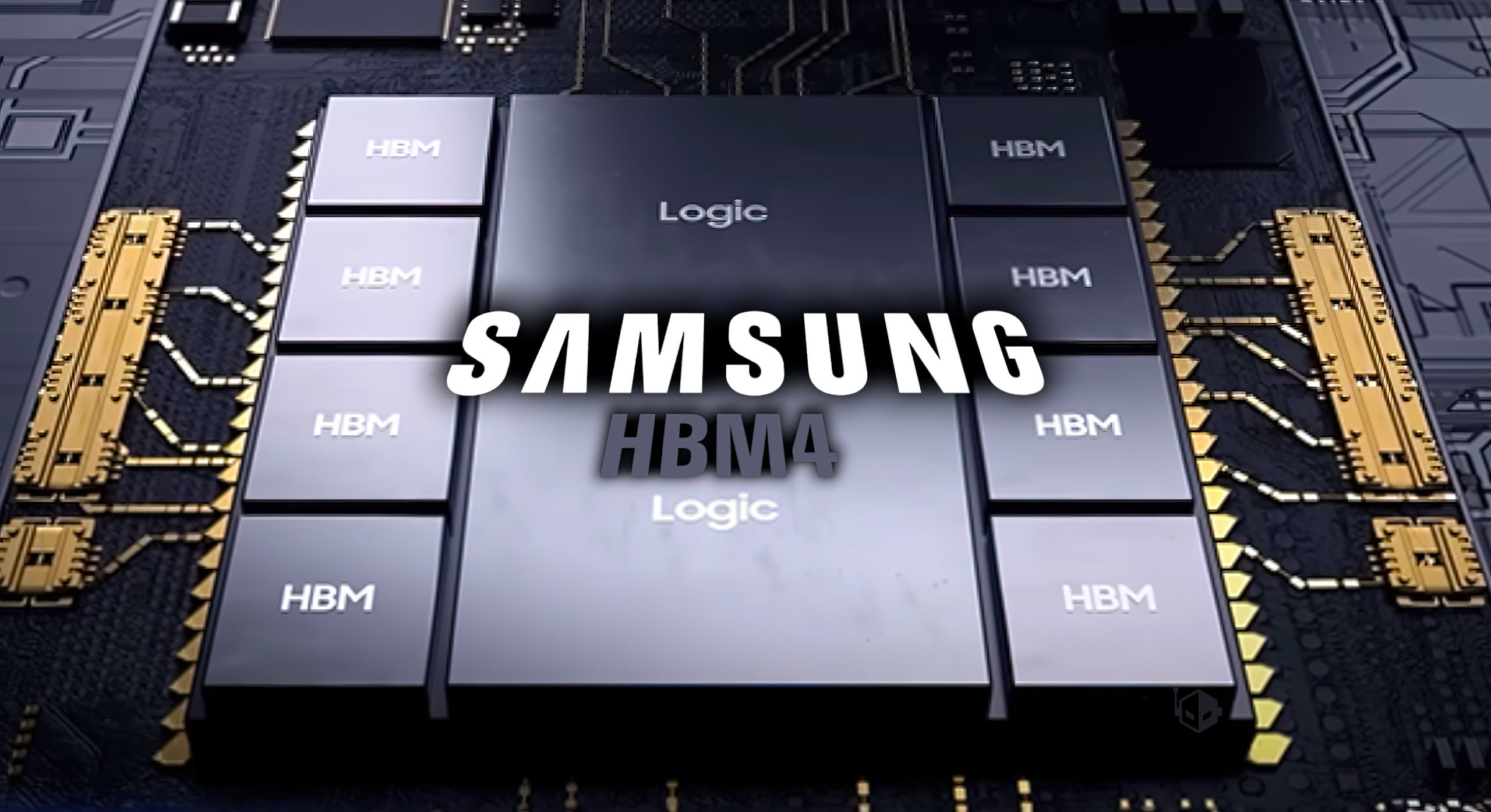
Samsung is putting its foot on the gas in high-bandwidth memory, unveiling major progress on HBM4 and HBM4E at the OCP Global Summit. The company’s next-gen HBM4E is targeting up to 13 Gbps per pin, translating to roughly 3.25 TB/s of bandwidth per stack—one of the fastest figures publicly discussed to date. Power efficiency is also set for a big leap, with Samsung claiming nearly double the efficiency of today’s HBM3E.
The roadmap doesn’t stop at HBM4E. Samsung says its HBM4 development has already hit 11 Gbps per pin, outpacing early industry targets and positioning the company to meet surging demand from AI and HPC customers. That push aligns with requests from major chipmakers to accelerate HBM4-class solutions to feed next-gen architectures, including NVIDIA’s Rubin.
There’s a strategic business play here as well. With a critical portion of HBM4 using on-package logic built on advanced 4 nm technology, Samsung can leverage its own foundry to streamline manufacturing and sharpen pricing. Reports suggest the company is willing to keep margins tight to win share, intensifying competition with SK hynix and Micron for future AI accelerator and data center wins.
Why this matters:
– AI training and inference depend on extreme memory bandwidth and capacity; HBM4E’s projected 3.25 TB/s per stack and improved efficiency can lift GPU and accelerator performance while lowering power per watt of bandwidth.
– Faster pin speeds—11 Gbps for HBM4 and up to 13 Gbps for HBM4E—help remove memory bottlenecks that limit large-scale model training and high-throughput workloads.
– A more aggressive pricing strategy could reshape supply dynamics for next-gen accelerators from companies like NVIDIA and AMD.
Availability timelines point to early 2026 for HBM4E, alongside mass production of HBM4. If Samsung delivers on these targets, the next wave of AI hardware could see substantial gains in bandwidth, efficiency, and total cost of ownership—right when the industry needs them most.