In a groundbreaking move within the realm of semiconductor manufacturing, Elephantech, a Tokyo-based company specializing in printed electronics, has unveiled an innovative inkjet technology named NeuralJet™. This AI-powered tech promises to revolutionize precision in semiconductor packaging, cleverly correcting printing variations and catering specifically to the demanding needs of advanced semiconductor production, including those utilized in artificial intelligence applications.
As the quest for ever-smaller components hits the boundaries of physical limitations in two-dimensional designs, the semiconductor industry is increasingly exploring three-dimensional stacking. Traditional methods such as spin coating struggle with the intricate requirements of 3D packaging, leading manufacturers to search for more versatile and precise alternatives.
Elephantech has risen to the challenge with their ELP04 device, which leverages NeuralJet technology to achieve single-drop ink placement precision. This remarkable system delivers coatings with a surface roughness (Ra) of just 0.8 nanometers, offering unparalleled control over film thickness from sub-micrometer to multiple micrometers. Such precision empowers manufacturers with the ability to apply bonding materials at precisely varied thicknesses, adapting to diverse application needs.
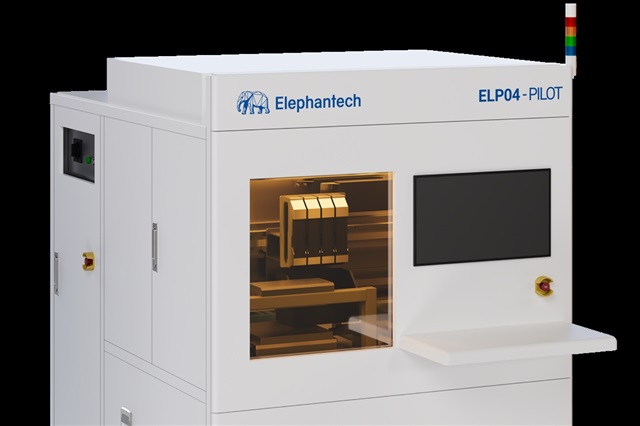
Moreover, Elephantech is expanding its offerings with the ELP04-PILOT, a compact inkjet system specifically geared for advanced packaging processes. This system supports the development of materials and optimization processes, with exciting potential uses in fields such as silicon photonics and the coating of heterogeneous materials.
According to Elephantech, this advancement marks a pivotal step forward in semiconductor manufacturing. With enhanced efficiency and meticulous precision, the technology is poised to broaden the horizons for AI semiconductor production and sophisticated packaging methods.
The potential applications of this technology are impressive, including the creation of high-heat-resistant adhesive coatings on wafers and the bonding of disparate materials like glass and silicon. The system excels in offering thickness control, selective patterning, and coating capabilities on non-uniform surfaces, all essential for effective 3D packaging.
This development underscores the industry’s commitment to improving semiconductor production processes, striving for greater efficiency while aiming to minimize environmental impact. As semiconductor designs continue to evolve, NeuralJet technology seeks to address the pressing challenges in packaging, fueling further advancements in the exciting world of semiconductor innovation.