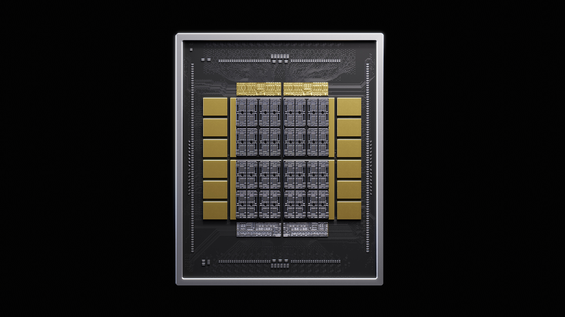
NVIDIA NVHBM promises faster, more efficient memory for future AI GPUs
NVIDIA has introduced NVHBM, a custom high-bandwidth memory technology designed to improve the performance and efficiency of future AI accelerators and GPUs. The new memory approach is built for the next generation of artificial intelligence workloads, where massive models, agentic AI systems, and physical AI applications are pushing memory bandwidth requirements to new levels.
As AI models continue to grow into the trillion-parameter range, memory has become one of the biggest bottlenecks in accelerator design. More compute power alone is not enough if data cannot move quickly and efficiently between memory and processing cores. NVIDIA’s NVHBM aims to solve that problem by rethinking how high-bandwidth memory connects to the main processor.
NVHBM is an extension of NVIDIA’s NVLink Fusion strategy, which is designed to connect GPUs, custom AI chips, and other accelerators into high-performance rack-scale systems. With NVHBM, NVIDIA is focusing on improving DRAM bandwidth, reducing power consumption, and freeing up valuable chip space for more compute resources.
The key change is where the memory controller is placed. In a traditional HBM design, the memory controller sits on the main accelerator chip, also known as the XPU. With NVHBM, NVIDIA moves the memory controller into the base die of the HBM stack itself. This shift allows the memory system to become more efficient while reducing the burden on the main compute die.
According to NVIDIA, this design can deliver more than 30% higher memory bandwidth compared with standard HBM4E. It can also reduce HBM power usage by up to 15%, which is especially important for large AI data centers running thousands of accelerators at once. Even small efficiency gains can translate into major savings when deployed at hyperscale.
Another major advantage is die area savings. By removing the memory controller from the XPU, NVIDIA says NVHBM can free up as much as 25% of the main chip area. That extra space can be used for additional compute capabilities, helping future GPUs and AI accelerators deliver more performance without simply increasing chip size.
The design also reduces the physical interface and supporting area needed for memory communication. Compared with the JEDEC HBM4E standard, NVIDIA says NVHBM can cut PHY and support area by up to 67%. A narrower interface also makes interposer routing less complex, potentially providing up to 80% more usable silicon across the full package layout.
These improvements matter because advanced AI chips are becoming increasingly constrained by packaging, power, and memory bandwidth. As accelerators grow larger and more complex, chipmakers need ways to increase performance without making designs harder to manufacture or more power-hungry. NVHBM is NVIDIA’s answer to that challenge.
NVIDIA is also working to make NVHBM a broader platform technology rather than a one-off custom implementation. The company plans to establish a standard NVHBM design that can be supported by multiple memory suppliers. This could help reduce engineering complexity for companies building custom AI accelerators and speed up the process of bringing new chips to market.
Amazon’s Annapurna Labs is one of the first major partners involved with NVHBM. The two companies are collaborating on integrating NVHBM technology with NVLink-based scale-up architectures to improve AI infrastructure performance and efficiency. Future AWS Trainium chips, beginning with Trainium4, are expected to use NVLink Fusion to connect Amazon’s custom AI silicon with NVIDIA GPUs in a shared rack-scale system.
This partnership highlights a larger trend in AI hardware: cloud providers and chip companies are increasingly building customized infrastructure instead of relying only on standard server designs. By combining custom AI chips, NVIDIA GPUs, NVLink Fusion, and NVHBM, future systems could deliver faster training and inference performance for large-scale AI models.
NVIDIA has already discussed custom HBM for its future Feynman GPU generation, which is expected to arrive around 2028. That makes Feynman a likely candidate to be among the first GPU architectures to adopt NVHBM. If the technology performs as claimed, it could become a major part of NVIDIA’s next wave of AI hardware.
For data centers, the benefits are clear: higher memory bandwidth, lower power consumption, more room for compute logic, and simpler chip packaging. For AI developers and cloud customers, this could mean faster model training, more efficient inference, and better performance for demanding workloads such as generative AI, robotics, simulation, and autonomous systems.
NVHBM shows that the future of AI performance will not depend only on faster GPUs. Memory architecture is becoming just as important. By redesigning how HBM works at the package level, NVIDIA is preparing its future accelerators for an era where moving data efficiently may be the key to unlocking the next leap in artificial intelligence computing.