When most people hear “computer memory,” they picture RAM or the storage inside a phone or laptop. In reality, memory is an entire family of semiconductor technologies, each built to solve a different problem. Some types are engineered for raw speed so a processor can work without waiting. Others are designed to keep your data safe even when the power is off. And because no single memory technology can be simultaneously blazing fast, ultra-cheap, high-capacity, low-power, and permanent, modern computers rely on a layered mix of memory types working together.
This guide focuses on four major memory technologies used across today’s devices: ROM, DRAM, SRAM, and flash memory. Understanding what each one does—and the trade-offs behind them—helps explain everything from why a CPU needs cache, to why programs load into RAM, to why SSD performance can vary under heavy use. It’s also practical knowledge if you’re comparing DDR5 kits, building a gaming PC, shopping for a new laptop, or simply trying to make sense of the performance specs thrown around in hardware discussions.
What memory really is
At the most fundamental level, computer memory stores information as bits—zeros and ones. That information might be actively used by a CPU, GPU, or other processor, or it may be kept long-term for the user in the form of apps, games, photos, and system files. Even though the physical reality is bits, memory capacity and performance are usually discussed in bytes (eight bits per byte), because that aligns better with how software and data are structured.
But “memory” doesn’t describe one single component. It’s a hierarchy of different storage layers that balance speed, capacity, cost, and reliability—because one technology can’t optimize every metric at once.
Volatile vs. non-volatile memory: the biggest divide
One of the most important ways to classify memory is whether it keeps data when power is removed.
Volatile memory needs constant electrical power to hold data. If the system shuts down, the data disappears. The upside is speed: volatile memory is typically used where quick read/write access is essential. DRAM and SRAM fall into this category.
Non-volatile memory retains data even with no power. That makes it ideal for firmware and long-term storage. ROM and flash memory are key examples of non-volatile memory in modern electronics.
Access patterns also matter: random vs. sequential
Another concept that shapes performance is how data can be accessed.
Random access means any location can be reached in roughly the same amount of time. This is where RAM gets its name: Random Access Memory. It’s a huge reason RAM is so effective for active computing.
Sequential access means data is most efficiently read in order. Some older storage systems are built around this idea, and while modern storage has improved significantly, access patterns still influence real-world performance and responsiveness.
Why computers use a memory hierarchy instead of “one perfect memory”
Modern systems combine multiple memory layers so each part of the machine gets what it needs without making everything extremely expensive. A simplified view looks like this:
Registers are tiny, extremely fast storage locations inside a CPU core (and similarly inside GPU compute units). They’re built for immediate, constant use.
Cache memory sits very close to the processor and is made from SRAM. It stores frequently used data so the CPU doesn’t have to wait on slower memory.
Main memory is DRAM. It’s much larger than cache and serves as the primary workspace for running applications and the operating system, but it has higher latency than SRAM.
Non-volatile storage is where long-term data lives—operating system files, installed programs, personal content, and games. Flash-based storage is the most common in modern devices.
This layered design exists largely because processors have historically improved faster than memory. If a fast CPU had to constantly wait for slow memory access, performance would collapse. This mismatch is often described as hitting a “memory wall,” and it’s a major reason cache and smart memory management are so important.
The core properties engineers care about
When comparing memory technologies, a few key measurements define their strengths and weaknesses:
Speed: how quickly reads and writes happen
Latency: the delay between asking for data and getting the first response
Bandwidth: how much data can be moved per second
Capacity: how much can be stored
Cost per bit: how expensive the memory is to manufacture at scale
Persistence: whether data survives a power loss
Energy usage: crucial for battery-powered devices and thermal limits
Every memory type is a compromise. Some deliver incredible speed but are expensive and small. Others offer huge capacity and persistence but can’t match RAM for responsiveness.
Why this affects everyday performance
These differences aren’t just academic—they shape how your devices feel.
When you launch an application, it typically loads from non-volatile storage into DRAM so the CPU can work on it quickly. This is why having enough RAM matters for multitasking and why systems bog down when memory runs out.
CPUs rely heavily on SRAM-based caches because software tends to reuse nearby data and recently used information. Cache helps avoid the latency penalty of reaching out to DRAM repeatedly.
Your files and installed games live in non-volatile storage like flash memory because it retains data even when your device is off. That permanence comes with different performance and endurance characteristics than RAM.
With that foundation in place, the next step is understanding how the four major memory types fit into real systems—starting with ROM, the non-volatile memory traditionally associated with firmware and the earliest steps of the boot process.
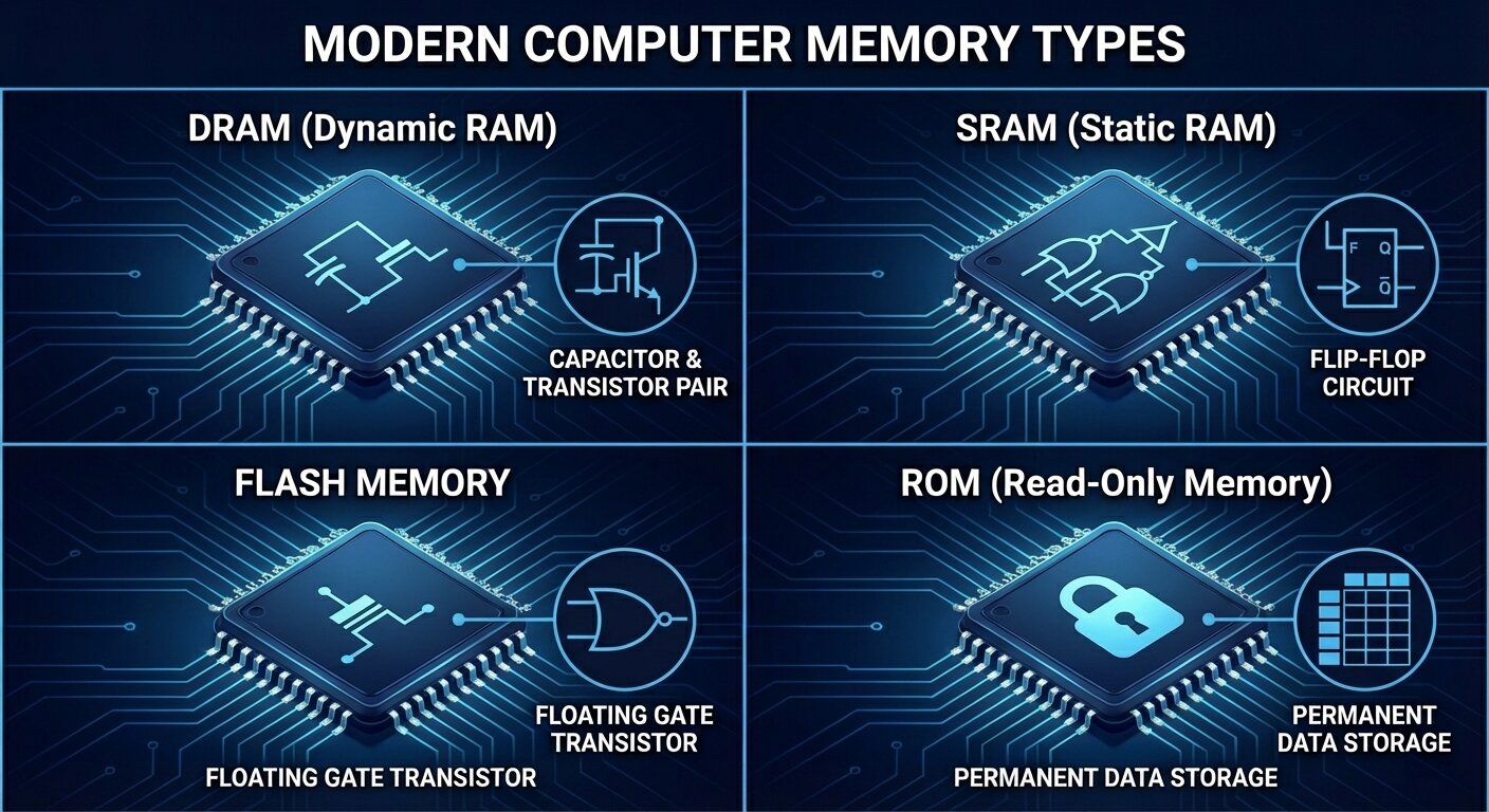
ROM (Read-Only Memory): the stable foundation for firmware
In modern computing, ROM refers to a broad category of non-volatile memory used to store essential, long-lived instructions that must survive power cycles. Historically, ROM literally meant memory that was written once and then only read. Over time, the term expanded in everyday usage as technology evolved, and many systems now use ROM-like storage that can be updated occasionally—especially for firmware.
ROM’s core purpose is reliability. It stores code a device needs to start up and operate correctly, such as boot instructions and low-level firmware. On PCs, the firmware environment (commonly referred to as BIOS or UEFI) has traditionally been stored in ROM. Many embedded systems—controllers inside appliances, electronics modules, and specialized devices—also depend on ROM to hold stable onboard software.
The key idea is that ROM isn’t designed for constant rewriting like RAM. Even when updates are possible, ROM-class storage is generally intended to be changed rarely, keeping critical startup and control code consistent and available every time the device powers on.As computers and electronics have evolved, “ROM” (read-only memory) hasn’t stayed stuck in a single, unchanging form. Over time, multiple ROM subtypes emerged to balance a core tradeoff: how permanent you want stored data to be versus how easily you need to update it. Some ROM types are essentially set in stone at the factory, while others can be erased and rewritten electrically inside a finished device.
Classic ROM subtypes, from most permanent to most flexible
Mask ROM (MROM): factory-programmed and unchangeable
Mask ROM is written during chip manufacturing. The data pattern is physically built into the silicon using custom photomasks, so the contents are effectively “hard-wired.” Once made, it can’t be updated.
Why it’s used: It’s extremely stable, fast to read, and becomes very cost-effective at huge production volumes since you avoid post-manufacturing programming steps.
Downside: It’s inflexible—any update requires producing a new mask and running a new fabrication batch, which is expensive and slow.
Common uses: Classic game cartridges, older consoles, and embedded systems with code that never needs updates.
PROM (Programmable ROM): one-time programmable
PROM ships blank, then a user programs it once using a PROM programmer. Programming typically works by “burning” internal fuses to lock bits into place permanently.
Why it’s used: It enables customization without requiring special factory masks, which is helpful when you want to finalize firmware late in the manufacturing process.
Downside: You only get one attempt—errors often mean the chip is wasted.
Common uses: Industrial embedded devices, early test setups, and application-specific logic where updates aren’t expected.
EPROM (Erasable Programmable ROM): UV-erasable and reprogrammable
EPROM improved on PROM by allowing reuse. Instead of being permanently fused, EPROM stores bits using floating-gate transistors. To erase it, you expose the chip to strong ultraviolet light through the familiar quartz “window” on top, which resets the stored charge so it can be programmed again.
Why it’s used: Great for iteration during development—engineers could update firmware repeatedly without tossing chips. It also became a familiar option for legacy BIOS storage.
Downside: Erasing is inconvenient in the real world. You generally must remove the chip from the device and place it under UV light. The process also isn’t ideal for frequent field updates.
Common uses: Older development boards and early microcontroller firmware workflows.
EEPROM (Electrically Erasable Programmable ROM): byte-level electrical updates
EEPROM takes the convenience of EPROM and brings it into normal operation: it can be erased and rewritten electrically without removing the chip. That makes it far better suited to devices that need configuration updates or occasional firmware changes.
What makes EEPROM stand out: It can typically rewrite individual bytes (byte-level erase/write), whereas flash memory usually erases and writes in larger blocks.
Why it’s used: You can update it in-system over common interfaces like SPI or I²C, making it practical for storing device settings, calibration values, and small firmware changes.
Downside: Write endurance is limited—often ranging from tens of thousands up to millions of cycles depending on the chip and usage patterns.
Common uses: BIOS/UEFI storage on many systems, microcontroller-based products, smart cards, security tokens, and persistent configuration storage.
Quick comparison of ROM types (what to remember)
Mask ROM: not programmable, not reprogrammable; locked at the factory; ideal for mass-produced fixed firmware.
PROM: programmable once, not reprogrammable; set by fuse burning; good for stable devices needing late-stage customization.
EPROM: programmable and reprogrammable; erased with UV light; common in older development and legacy firmware.
EEPROM: programmable and reprogrammable; electrically erasable (often byte-level); ideal for BIOS, microcontrollers, and configuration data.
DRAM explained: the main memory your computer actually works in
While ROM focuses on storing firmware and persistent data, DRAM (Dynamic Random-Access Memory) is the workhorse memory used as main system memory in most modern computers, servers, and many other devices. DRAM stores each bit as electrical charge in a tiny capacitor. The problem: that charge leaks over time. So DRAM has to be refreshed constantly—hundreds of times per second—to keep data intact. This “dynamic” refresh requirement is where DRAM gets its name.
Why DRAM dominates: Compared with SRAM, DRAM cells are simpler (typically one capacitor and one transistor per bit), so manufacturers can pack far more memory into the same chip area. The result is much higher density and a much lower cost per gigabyte, which is exactly what systems need for large amounts of working memory.
How DRAM works at a practical level
DRAM is arranged like a grid of rows and columns:
Word lines (rows) act like selectors. When the memory controller activates a word line, it enables access to an entire row of cells at once.
Bit lines (columns) carry data to and from the cells and connect to sense amplifiers that detect tiny voltage changes.
Reading data: The bit line is precharged to an intermediate level, the row is activated, and the small charge in a cell slightly shifts the bit line voltage. A sense amplifier detects and amplifies that tiny difference to determine whether the bit is a 1 or a 0.
Writing data: The system drives the bit line strongly to a 1 or 0 and activates the row so the capacitor is charged or discharged accordingly.
A key detail: reading DRAM is “destructive” in the sense that the act of reading disturbs the stored charge, so the memory system must restore the value afterward. Combined with natural charge leakage, this is why refresh operations are essential.
DRAM strengths and weaknesses (why it’s great, and what it costs)
Strengths: High density at reasonable cost, strong bandwidth for general-purpose workloads, and broad standardization across DDR generations.
Weaknesses: It must refresh (consuming power), it’s volatile (loses data without power), and it has higher access latency than SRAM, especially for random access patterns.
Typical uses: Main system memory in desktops, laptops, phones, servers, and workloads where capacity and cost matter—everything from everyday applications to virtualization and large datasets.
Memory buses: how the CPU and memory communicate
Even the fastest memory is useless if the system can’t move data efficiently. That’s where the memory bus comes in: a set of electrical pathways and signaling rules that connect the processor (more specifically, the memory controller) to DRAM and other memory devices. Modern systems implement these connections as high-speed standardized interfaces designed to move data quickly and reliably.
A memory bus is usually described in three parts:
Address bus: tells memory which location the CPU wants to access. The width of the address bus helps determine how much memory can be addressed.
Data bus: carries the actual data back and forth. Wider data buses can move more bits per transfer, boosting bandwidth.
Control bus: carries command and timing signals (such as read or write) that coordinate how and when transfers happen.
Together, these buses form the core “highway system” for memory operations, enabling the CPU to fetch instructions and data from DRAM and to store results back into memory.The width of a memory bus (how many lines can move data in parallel) and its speed (the operating frequency) play a huge role in how much information a system can push back and forth every second. In other words, they directly shape memory bandwidth. A simple way to picture it is a highway: more lanes and higher speed limits move more cars in less time.
Today’s computers don’t rely on the old “front-side bus” model that many people remember from earlier PC eras. Instead, modern platforms use more specialized, point-to-point memory interfaces that are tightly integrated into the CPU’s memory controller and defined by standards such as DDR, LPDDR, GDDR, and HBM. Even though the wiring and signaling have evolved significantly, the fundamentals are the same: a memory controller sends commands, selects addresses, transfers data, and manages timing across dedicated physical lines.
DRAM vs. SDRAM: why the “DRAM” in your PC is almost always SDRAM
People commonly say “DRAM” when talking about system memory, but practically all modern DRAM chips are actually SDRAM, which stands for Synchronous Dynamic Random-Access Memory. The key difference is right in the name: SDRAM operates in sync with a clock signal.
Older asynchronous DRAM didn’t coordinate its command and data operations to the same clock in a tightly controlled way. SDRAM does, meaning the memory controller (the logic that manages reads, writes, refresh behavior, and flow of data between the CPU and RAM) and the memory chips operate in lock-step timing. That synchronization is what enables major performance-boosting techniques like command pipelining and bank interleaving, both of which help keep data flowing efficiently instead of forcing the system to “wait around” between operations.
This is why the popular memory families you see today—DDR, LPDDR, GDDR, and even HBM—are all built on an SDRAM foundation. They differ in goals (bandwidth, power efficiency, latency, or specialized workloads), but they share that same synchronous core design.
Understanding memory timings (and why the numbers matter)
If you’ve ever shopped for DDR memory and seen a string like “30-36-36-76,” you were looking at the primary memory timings. These numbers represent delays measured in clock cycles—how many ticks the memory needs to complete important internal operations.
Because DRAM is structured like a grid of rows and columns, accessing data is not as simple as grabbing a value instantly. The memory typically needs to open (activate) a row, then read or write a column inside it. Each step introduces a specific delay. The most commonly discussed timings include:
CAS Latency (tCL): The delay, in clock cycles, between issuing a read command and getting the data back, assuming the correct row is already open. This is the timing most people recognize first and is often treated as shorthand for responsiveness.
Row-to-Column Delay (tRCD): The time between opening a row and being able to access a column within that row. Think of it as the “row setup” delay before the data in that row can be used.
Row Precharge Time (tRP): Before the memory can switch from one row to another, it has to close the current row. tRP measures how long that “close and reset” step takes.
Row Active Time (tRAS): The minimum time a row must remain open after activation to ensure operations complete safely before it can be closed again.
Lower timing numbers generally mean fewer clock cycles of waiting, which can translate to lower latency. But real latency depends on both timings and frequency. A kit with tighter timings at a lower speed can end up similar in actual nanosecond delay to a faster kit with looser timings. That’s why serious performance comparisons often look beyond a single timing number and consider the full combination of data rate and latency.
Primary timings also aren’t the whole story. Beneath them are secondary and tertiary timings—additional parameters that control more detailed behaviors, including how DRAM handles specific command sequences, refresh operations, and edge-case access patterns. These subtimings usually aren’t printed on the box, but they can often be viewed (and sometimes tuned) in BIOS/UEFI settings. For enthusiasts, targeted subtiming tuning can sometimes deliver bigger real-world gains than simply tweaking the headline timings, especially after frequency goals have already been reached.
The major modern DRAM types you’ll see today
Not all “RAM” is built for the same job. Modern systems typically rely on a few major DRAM families, each optimized for different priorities like power draw, bandwidth, size, and cost.
DDR (Double Data Rate): the standard system memory for PCs and servers
DDR is the mainstream RAM used in desktops, laptops, workstations, and servers. Its defining trait is that it transfers data on both the rising and falling edges of the clock signal, effectively doubling the data rate per cycle compared to older single data rate designs. Over multiple generations—from DDR1 through DDR5, with future standards already on the horizon—DDR has steadily improved in speed, capacity, and power efficiency.
Why DDR is popular:
It delivers balanced performance across bandwidth, latency, and capacity, making it suitable for a wide range of everyday computing tasks.
It’s widely supported and typically easy to upgrade thanks to standardized modules like DIMMs.
It remains cost-effective due to mature manufacturing and broad adoption, and it’s far cheaper and denser than SRAM.
Where DDR falls short:
It’s not as power-optimized as mobile-focused memory types.
It has much higher latency and far lower bandwidth than SRAM, which is why CPUs rely heavily on caches rather than trying to use DRAM for everything.
Where you’ll find it:
General-purpose system memory in consumer and enterprise desktops, laptops, and servers.
LPDDR (Low-Power DDR): memory designed for efficiency-first devices
LPDDR is built for battery-powered and mobile hardware like smartphones, tablets, and thin-and-light laptops. It uses the same underlying DRAM technology as DDR, but prioritizes energy efficiency through lower operating voltages and additional power-saving states designed for always-on, mobile-style usage.
A major design difference is packaging and integration. In many devices, LPDDR is soldered directly onto the motherboard rather than placed in removable modules. That enables smaller, thinner designs and can improve power characteristics by shortening signal paths.
Why LPDDR is favored in portable devices:
Excellent energy efficiency for longer battery life.
Strong support for low-power idle and always-on behaviors without excessive drain.
Space-saving design choices that help manufacturers build slimmer devices.
Trade-offs to know:
It’s usually not upgradeable because it’s soldered down.
Latency is often higher than standard DDR due to looser timings.
Where you’ll find it:
Smartphones, tablets, ultra-portable laptops, and many embedded and automotive systems.
GDDR (Graphics DDR): bandwidth-hungry memory for GPUs and parallel workloads
GDDR is a specialized memory type designed to push very high bandwidth, which is why it’s commonly used with graphics processors. Like LPDDR, it’s typically soldered onto the device board rather than installed as user-upgradable modules. GDDR reaches high throughput through high data rates and wide memory buses, making it well-suited for rendering, gaming, and other massively parallel workloads where memory bandwidth can be a primary performance limiter.
Why GDDR stands out:
Very high data rates to move large blocks of data quickly between GPU and memory.
Well-suited to parallel workloads, especially when paired with multiple memory channels to maximize throughput.
The trade-off:
GDDR tends to prioritize raw speed over power efficiency, which is acceptable for performance-focused GPUs and accelerators but less ideal for ultra-low-power devices.When people talk about “memory,” they’re often lumping together several very different technologies that each target a specific job. Some types are built to move huge amounts of data every second, others focus on low power for portable devices, and a few are designed purely for speed even if they’re expensive and limited in capacity. Here’s a clearer, more practical look at the major memory types covered in your content—especially the high-bandwidth DRAM families, SRAM, and the basics of flash memory.
GDDR (Graphics Double Data Rate) is the go-to memory for graphics-heavy workloads where raw throughput matters most. It’s engineered to feed GPUs with extremely high bandwidth by running at very high operating frequencies and using wider memory buses. That design choice is exactly why it shows up in graphics cards, gaming consoles, and professional visualization hardware where large textures, frame buffers, and rendering workloads demand fast data movement.
The trade-off is that pushing frequency and bus width comes with real thermal and electrical costs. GDDR can generate more heat and draw more power than general-purpose system memory, which is why cooling and board design are such a big deal on high-end GPUs. It’s also not meant to be “universal” memory—the architecture leans hard into bandwidth rather than optimizing for latency or flexibility, making it a specialist rather than an all-around solution.
HBM (High Bandwidth Memory) takes the idea of bandwidth optimization even further, but with a completely different physical approach. Instead of spreading memory chips out across a board and connecting them over longer traces, HBM stacks DRAM dies vertically into a compact package and uses Through-Silicon Vias (TSVs) plus an ultra-wide interface to move data at enormous rates. The end result is massive throughput per package—often hundreds of gigabytes per second per stack—while also improving energy efficiency per bit transferred compared with DDR and GDDR.
A key part of HBM’s performance comes from how it’s integrated. HBM is typically paired with high-performance GPUs, AI accelerators, or HPC processors using a 2.5D package. In this arrangement, the processor die sits alongside one or more HBM stacks on an interposer, a thin intermediary substrate designed to route thousands of dense, high-speed connections with short paths. Those short interconnects help reduce power loss and support extremely wide data interfaces that would be impractical on a standard PCB.
HBM’s strengths are clear: exceptional bandwidth, excellent energy efficiency, and a dense form factor that enables high-performance designs in less space. The downside is equally clear: it’s expensive and complex to manufacture due to TSVs, interposers, and advanced packaging. Capacity can also be more limited than standard DRAM configurations because the focus is on throughput rather than maximizing sheer memory size. That’s why HBM is commonly found in AI accelerators (including GPU and TPU-class devices) and high-performance computing systems where bandwidth and efficiency directly translate to real-world performance.
If you compare common DRAM types at a glance, the “why” behind each one stands out. DDR is the balanced, cost-effective choice for mainstream desktops, laptops, and servers. LPDDR is tuned for energy efficiency in phones, tablets, and thin-and-light devices, often with higher latency and limited upgradeability as trade-offs. GDDR targets sheer throughput for GPUs, accepting higher heat and power draw. HBM aims for extreme bandwidth with strong efficiency, but demands costly, complex packaging—making it a premium tool for AI and HPC.
SRAM (Static Random-Access Memory) sits in a different category altogether. It’s still volatile memory (data disappears without power), but it’s used where speed and predictability matter more than capacity or cost. The big difference is how it stores data. DRAM relies on electrical charge in capacitors and needs periodic refresh cycles to keep data intact. SRAM uses transistor-based flip-flops—commonly a six-transistor (6T) cell—that can hold a stable 0 or 1 as long as power is supplied, with no refresh required.
That design gives SRAM several standout characteristics. Access times can be extremely fast, commonly in single-digit nanoseconds—often far quicker than DRAM, which typically lands in the tens of nanoseconds. With no refresh cycles, SRAM avoids latency interruptions and reduces background energy spent on maintenance. It’s also valued for deterministic timing, meaning performance is more predictable—an advantage in real-time systems and performance-critical logic.
These benefits come with major drawbacks. SRAM is expensive per bit because each bit requires multiple transistors, and it’s less dense because those transistors take up significant silicon area. That makes SRAM impractical for large memory pools. You’ll usually find SRAM in roles like CPU and GPU caches (L1, L2, L3), register files, small buffers inside processors, high-speed packet buffering in networking hardware, and embedded or real-time systems that can’t afford unpredictable memory delays. Many FPGAs also include SRAM-based block RAM for fast, configurable on-chip storage.
Finally, flash memory is introduced as a different kind of storage altogether: non-volatile solid-state memory that keeps data even when power is removed. It evolved from earlier non-volatile technologies like EEPROM, with key development credited to Fujio Masuoka at Toshiba in the 1980s. While RAM types like DDR, GDDR, HBM, and SRAM are primarily about fast working data for active computation, flash is designed for persistence—holding information long after a device powers down.
If you’d like, I can rewrite the remaining flash memory section as well once you paste the rest of that portion of the source content (it cuts off mid-sentence here).Flash memory is built around a simple but powerful idea: store data even when the power is off, and do it cheaply enough to scale from tiny embedded devices to massive data centers. Unlike volatile memory such as DRAM or SRAM, which forget everything the moment electricity stops flowing, flash memory keeps information by trapping electrical charge inside floating-gate transistors. With no moving parts, it delivers fast access, strong durability, and excellent energy efficiency compared with traditional hard drives.
Over time, flash split into two main families that share the same floating-gate origins but behave very differently in real-world systems: NOR flash and NAND flash. Understanding the difference helps explain why your SSD uses one type, while many devices still rely on the other for critical startup code.
NOR vs NAND flash: the core difference
The “NOR” and “NAND” names come from how memory cells are connected.
NOR flash uses a parallel-style connection that allows direct access to individual memory addresses. That means a system can read small chunks of data quickly and predictably.
NAND flash chains cells in a series-style arrangement. This design is optimized for packing in as much storage as possible and moving data efficiently in pages and blocks, rather than focusing on tiny byte-by-byte access.
That single architectural choice ripples through everything else: performance profile, cost per gigabyte, endurance behavior, and where each type makes the most sense.
NOR flash memory: where fast random reads matter most
NOR flash is often chosen when a device needs dependable, low-latency random reads and the ability to run code straight from the flash chip.
Key strengths of NOR flash
Fast random access at the byte level, which is ideal for execute-in-place (XIP) scenarios where firmware can run directly from flash
Reliable reads, thanks to the parallel structure that simplifies access patterns
Often stronger endurance and longer data retention in smaller-capacity uses compared with NAND
Main weaknesses of NOR flash
Lower storage density, because the parallel layout uses more chip area per bit
Slower erase and write operations, especially as capacity grows
Higher cost per bit, which is why it’s rarely used for large consumer storage
Common NOR flash use cases
Firmware and boot storage such as BIOS/UEFI and other boot ROM functions
Embedded systems and microcontrollers with relatively small code footprints
Applications that prioritize long retention and predictable random access over sheer capacity
NAND flash memory: the backbone of modern storage
If NOR is about precise random reads, NAND is about scale. NAND flash is the reason SSDs, memory cards, and phone storage can deliver huge capacities at consumer-friendly prices.
Key strengths of NAND flash
High density, enabling much larger capacities per chip
Efficient erase and write behavior at the block level, ideal for bulk data movement
Low cost per bit, driven by compact design and mass-market manufacturing
Main weaknesses of NAND flash
Slower random access than NOR because it operates on pages and blocks rather than individual bytes
More complex to manage, requiring controllers that handle error correction (ECC), wear leveling, and bad-block management
Lower per-cell endurance compared with NOR in many scenarios, with durability depending heavily on the NAND type used
Common NAND flash use cases
SSDs for PCs, laptops, and servers
USB flash drives and SD/microSD memory cards
Smartphone and tablet internal storage
Large-scale consumer and cloud storage where capacity and cost efficiency dominate
NAND cell types explained: SLC vs MLC vs TLC vs QLC
Not all NAND is the same. NAND stores bits by trapping charge at specific voltage levels. The more bits you store in a single cell, the more voltage levels the hardware must distinguish, and the more challenging it becomes to read and write accurately.
The main NAND cell types are:
SLC (Single-Level Cell): 1 bit per cell, simplest and most robust
MLC (Multi-Level Cell): 2 bits per cell, balances cost and performance
TLC (Triple-Level Cell): 3 bits per cell, higher density and lower cost
QLC (Quad-Level Cell): 4 bits per cell, highest mainstream density today
The practical trade-off is consistent as you move from SLC to QLC:
Capacity per chip increases
Cost per gigabyte goes down
Endurance (write-cycle lifespan) generally decreases
Raw performance, especially sustained write speed, tends to drop
In other words, higher-density NAND is fantastic for affordable capacity, but it typically needs more clever controller tech and caching strategies to feel fast and last long under heavy write workloads.
How NOR and NAND compare at a glance
NOR flash typically delivers true random byte access and fast random reads, but it’s more expensive and tops out at lower capacities. NAND flash is designed for page and block access, excels at high-capacity storage with strong sequential performance, and wins on cost per bit, but it relies on advanced controller features to handle errors and wear over time.
Why computers use a memory hierarchy instead of “one perfect memory”
No single memory technology offers maximum speed, maximum capacity, lowest cost, and non-volatility all at once. That’s why modern devices use a layered memory hierarchy.
At the top are tiny pools of ultra-fast volatile memory close to compute units (CPU, GPU, TPU), where speed matters most. SRAM serves as cache, DRAM serves as system memory, and then non-volatile technologies like flash provide persistent storage for operating systems, apps, files, and large datasets. This combination lets devices feel responsive while still offering durable long-term storage.
A simplified view looks like this:
ROM: non-volatile, slower, used for firmware and boot code
SRAM: volatile, extremely fast, used for caches and small buffers
DRAM: volatile, fast, used as system RAM and graphics memory
Flash: non-volatile, moderate speed, extremely dense and low cost, used for SSDs and other persistent storage
Future memory trends: what comes after today’s mainstream flash and DRAM
As AI, cloud computing, IoT, and data-heavy applications keep pushing hardware harder, the gaps in today’s memory systems become more obvious. The industry is exploring new approaches that improve bandwidth, reduce energy use, and narrow the distance between “working memory” and “storage.”
Z-Angle Memory (ZAM)
Z-Angle Memory is a stacked memory architecture under development to compete with high-bandwidth memory used in AI accelerators and high-performance computing. The goal is greater density, higher bandwidth, and improved energy efficiency to ease memory bottlenecks. Early timelines point toward commercialization around 2029–2030, with prototypes already appearing at industry events.
Magnetoresistive RAM (MRAM)
MRAM stores data using magnetic states rather than electrical charge. Its appeal is the rare mix of non-volatility, low latency, and high endurance. Variants such as STT-MRAM and SOT-MRAM are being developed to push performance closer to SRAM-like speeds, potentially enabling new designs where fast persistent memory plays a larger role.
The takeaway
NOR and NAND flash aren’t competing versions of the same thing so much as specialized tools built from the same core concept. NOR is ideal for reliable, fast random reads and firmware-style workloads, while NAND dominates modern storage because it scales to massive capacities at low cost. As computing demand continues to rise, new memory technologies are racing to complement or reshape today’s hierarchy—while flash remains a foundational piece of how devices store data reliably without power.The future of computer memory is being shaped by a simple goal: deliver DRAM-like speed without losing data when power is off, while also improving endurance and efficiency compared to today’s flash storage. Several next-generation memory technologies are moving closer to real-world use, each offering a different path toward faster, denser, longer-lasting non-volatile memory.
One of the most promising ideas is MRAM (Magnetoresistive RAM), a technology designed to deliver near-RAM performance while keeping the “persistence” people associate with flash storage. MRAM stores data using magnetic states rather than trapped electrical charge, which can dramatically improve durability and data retention. A recent development involving tungsten layers reportedly enabled switching speeds around 1 nanosecond, a major indicator of how MRAM could eventually function as ultra-fast non-volatile working memory. If these gains translate into scalable manufacturing, MRAM could help bridge the long-standing gap between high-speed system memory and long-term storage, with far greater longevity than flash.
Another fast-rising candidate is ReRAM (Resistive RAM), also known as RRAM. Instead of magnetism, ReRAM encodes data by changing the electrical resistance of a dielectric material. Its appeal comes from a relatively simple cell structure, low programming voltage, and fast switching behavior. ReRAM is also seen as highly scalable, with the potential to keep shrinking below 10 nm process nodes—an important advantage for building dense, high-capacity chips without ballooning cost or power. Industry activity suggests embedded ReRAM could arrive more broadly in areas like IoT devices, where low power and long endurance matter. Beyond storage, ReRAM also draws attention for analog computing and in-memory computation, making it especially interesting for AI accelerators and edge computing where moving data back and forth is a major efficiency bottleneck.
Phase-Change Memory (PCM) takes a different approach by using heat to toggle a chalcogenide material between amorphous and crystalline states. This lets PCM store data with much lower latency than NAND flash while improving endurance. Unlike DRAM, PCM doesn’t require refresh cycles to retain data, which can reduce energy waste in certain workloads. PCM can also use multiple intermediate states, enabling multi-bit storage in a single cell. While challenges remain—particularly around materials engineering, write energy, and scaling—ongoing research continues to push PCM toward a role as “storage-class memory,” sitting between DRAM and flash in both speed and persistence.
There are also experimental approaches that hint at even bigger leaps. Ferroelectric-based technologies such as FeFET-style flash and other ferroelectric concepts aim to bring polarization-based storage into NAND-like structures, potentially cutting power use while improving speed and endurance compared to traditional charge-trap flash. Meanwhile, Nano-RAM (NRAM), a concept based on carbon nanotubes, is often discussed as a way to deliver DRAM-like performance with non-volatility and very high density. These options are still earlier on the maturity curve, but they highlight how breakthroughs in materials science and device design could reshape how memory works at a fundamental level.
What all of this reinforces is that memory is not a single “part” of a computer—it’s an entire ecosystem. Modern systems rely on multiple memory types because each one involves trade-offs among speed, capacity, cost, endurance, and whether data persists without power. Traditional pillars such as ROM, DRAM, SRAM, and flash each play a specific role, and computers are designed as layered hierarchies to take advantage of their strengths while minimizing weaknesses.
Looking ahead, emerging non-volatile RAM technologies, along with advanced packaging and stacked memory architectures, could further blur the old boundaries between “memory” and “storage.” The next evolution of computing will be heavily influenced by how well these new memory technologies balance performance, persistence, and affordability—because the best future machines won’t rely on a single perfect memory type, but on smarter combinations that make the entire system faster, more efficient, and more resilient.